 ALLPCB


14 Aviation and Aerospace PCB Design Rules for High Reliability
Aviation and aerospace systems operate in environments that combine extreme temperatures, vibration, radiation, and pressure changes. Printed circuit boards in these applications must maintain electrical performance and mechanical integrity over long service lives. Aerospace PCB design guidelines therefore emphasize conservative margins, material stability, and rigorous process controls. Engineers apply these rules from the initial concept stage through final qualification to reduce the risk of in-flight failures.
Why Aviation and Aerospace PCB Reliability Matters
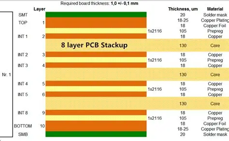
Aircraft and spacecraft electronics control flight surfaces, navigation, propulsion, and life support. A single board failure can compromise mission success or passenger safety. Aviation PCB stackup choices directly influence signal integrity, thermal dissipation, and resistance to mechanical stress. Consistent dielectric thickness and copper distribution help maintain performance when ambient conditions fluctuate rapidly. These factors drive the adoption of specialized design practices that exceed those used in commercial electronics.
Technical Principles Behind High-Reliability PCB Design
Coefficient of thermal expansion mismatch between copper, laminate, and components creates stress during temperature cycling. Controlled expansion materials and balanced copper distribution reduce warpage and via cracking. Vibration induces fatigue in traces, vias, and solder joints, so designers incorporate additional support structures and appropriate component anchoring. Electromagnetic interference from onboard systems requires careful return-path planning and shielding integration. Moisture ingress can degrade insulation resistance, making surface finishes and protective coatings essential considerations.
Fourteen Aviation and Aerospace PCB Design Rules for High Reliability
- Rule 1 requires selection of base materials with glass transition temperatures well above the maximum operating range and low coefficients of thermal expansion in the z-axis.
- Rule 2 specifies symmetric stackup construction to minimize bow and twist during thermal excursions.
- Rule 3 calls for minimum dielectric thickness between power and ground planes to achieve target impedance while maintaining adequate voltage isolation.
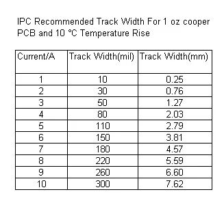
- Rule 4 mandates trace width calculations that include current cushioning factors beyond nominal operating loads.
- Rule 5 limits via aspect ratios and requires filled or capped vias in high-stress locations.
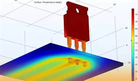
- Rule 6 directs placement of high-power components near thermal vias or copper pours sized for heat spreading.
- Rule 7 requires component derating according to temperature, voltage, and current guidelines established for aerospace environments.
- Rule 8 specifies mechanical reinforcement features such as edge stiffeners or underfill for large packages subject to vibration.
- Rule 9 incorporates conformal coating selection based on expected humidity and contamination levels.
- Rule 10 requires controlled-impedance routing with verified return paths for high-speed signals.
- Rule 11 limits the number of sequential lamination cycles to preserve material integrity.
- Rule 12 calls for redundant power distribution paths where single-point failures are unacceptable.
- Rule 13 specifies test points and fiducials that support in-process inspection without compromising reliability.
- Rule 14 requires documentation of all design assumptions and qualification test results for traceability.
Practical Implementation of the Design Rules
Engineers begin by defining the full environmental envelope, including temperature extremes, vibration spectra, and radiation exposure. Stackup planning follows, balancing signal layers, power planes, and dielectric thicknesses to meet both electrical and mechanical targets. Trace and via sizing incorporate current cushioning and thermal relief features. Component libraries include derated parameters, and placement routines prioritize thermal paths and mechanical support. After layout completion, simulation verifies impedance, thermal performance, and vibration response before fabrication release. Post-fabrication inspection follows acceptance criteria aligned with established industry specifications.
Quality and Process Controls Supporting the Rules
Fabrication and assembly processes must maintain the tolerances assumed during design. Laminate storage, drilling parameters, plating thickness, and surface finish application all receive documented controls. Assembly sequences include verification of component orientation, solder joint quality, and coating coverage. Environmental stress screening, such as thermal cycling and vibration, confirms that the finished assembly meets reliability targets before integration into higher-level systems.
Conclusion
Adherence to these fourteen rules produces printed circuit boards capable of sustained operation in demanding aviation and aerospace conditions. Systematic attention to material properties, stackup symmetry, thermal paths, mechanical reinforcement, and derating margins reduces failure risk. When combined with controlled manufacturing and verification processes, the resulting hardware supports the long-term performance expectations of the industry.
FAQs
Q1: What are the primary aerospace PCB design guidelines for ensuring long-term reliability?
A1: The guidelines focus on material stability, symmetric construction, adequate current and thermal margins, and mechanical reinforcement to withstand vibration and temperature cycling throughout the service life of aircraft or spacecraft systems.
Q2: How does aviation PCB stackup design contribute to overall system performance?
A2: A well-planned aviation PCB stackup controls impedance, manages heat flow between layers, and maintains dimensional stability, thereby supporting signal integrity and reducing stress on interconnects during flight conditions.
Q3: Why is dielectric thickness control important in aerospace PCB applications?
A3: Precise dielectric thickness maintains consistent electrical characteristics and voltage isolation while minimizing the risk of delamination or cracking when the board experiences repeated thermal and mechanical loads.
Q4: What role does current cushioning play in aerospace PCB trace width selection?
A4: Current cushioning provides additional margin beyond expected operating loads, allowing traces to handle transient surges and elevated temperatures without excessive heating or electromigration over extended mission durations.
References
IPC-6012E — Qualification and Performance Specification for Rigid Printed Boards. IPC, 2017
IPC-A-600K — Acceptability of Printed Boards. IPC, 2020
JEDEC J-STD-020E — Moisture/Reflow Sensitivity Classification. JEDEC, 2014


