ALLPCB


Printed Circuit Boards (PCBs) are the backbone of modern electronics, powering everything from smartphones to industrial machinery. For engineers, ordering PCBs is a critical step in product development, but even seasoned professionals can stumble into costly pitfalls. A single mistake in the ordering process can lead to delays, increased costs, or even product failure. In this blog, we'll explore the most common mistakes engineers make when ordering PCBs and provide actionable tips to avoid them, ensuring your project stays on track.
Whether you're designing a high-speed PCB for telecommunications or a compact board for a wearable device, understanding these errors can save time and resources. Let's dive into the key mistakes to steer clear of and how to address them effectively.
1. Inadequate Design for Manufacturability (DFM) Checks
One of the most frequent mistakes is neglecting thorough Design for Manufacturability (DFM) checks before submitting PCB files. DFM ensures your design aligns with the manufacturing capabilities of your PCB supplier. Without it, you risk issues like insufficient trace widths, improper component spacing, or unmanufacturable board dimensions.
For example, a common error is designing traces too narrow for high-current applications. Traces carrying currents above 500 mA require wider paths to prevent overheating—typically calculated using a trace width calculator to achieve, say, a 0.5 mm width for 1 A on a 1 oz copper layer. Ignoring this can lead to burnt traces or signal degradation. Similarly, components placed too close to the board's edge (e.g., less than 0.5 mm) may violate manufacturer tolerances, complicating assembly.
How to Avoid It: Always run DFM checks using tools like FreeDFM from Advanced Circuits or consult your manufacturer's guidelines. Review spacing, trace widths, and via placements early in the design phase. Partner with a fabricator who offers DFM feedback to catch issues before production begins.
2. Incorrect or Incomplete File Submissions
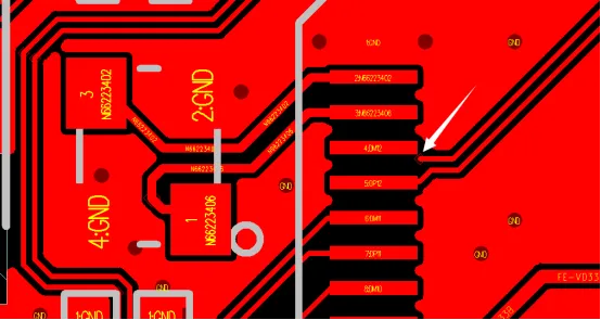
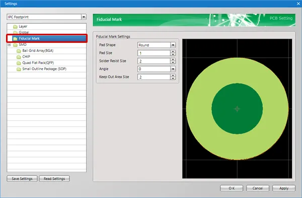
Submitting incomplete or incorrect files is a recipe for delays. PCB manufacturers typically require Gerber files, a Bill of Materials (BOM), pick-and-place files, and drill files. Missing files or errors in formatting—like omitting fiducial markers or using incorrect Gerber layers—can halt production or result in faulty boards.
A real-world example: an engineer might forget to include fiducial markers, which are essential for aligning surface-mount components during assembly. Without them, automated machines may misplace components, leading to a 10-20% yield drop in some cases. Similarly, a BOM lacking manufacturer part numbers can cause sourcing delays, especially for niche components like a 50-ohm RF connector.
How to Avoid It: Double-check your file package before submission. Ensure Gerber files are exported correctly (e.g., RS-274X format), include all necessary layers, and verify that the BOM lists reference designators, quantities, and part numbers. Use a checklist provided by your manufacturer to confirm completeness.
3. Ignoring Signal Integrity and Impedance Requirements
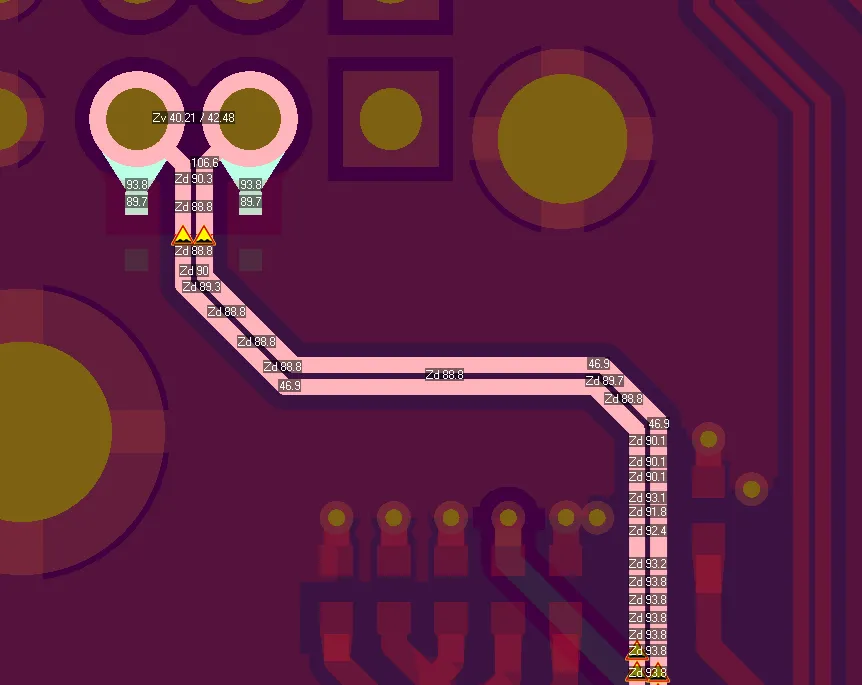
For high-speed PCBs, such as those used in 5G devices or DDR4 memory systems, neglecting signal integrity and impedance control is a critical error. Mismatched impedance can cause signal reflections, reducing performance or causing data errors. For instance, a 50-ohm microstrip transmission line requires precise trace width and dielectric thickness—often 0.15 mm wide on a 0.2 mm FR4 substrate for 50 ohms.
Another oversight is routing high-speed signals, like those exceeding 1 GHz, without considering trace length or differential pair matching. A length mismatch of just 5 mm in a 3 GHz signal can introduce a 50 ps delay, enough to disrupt timing in high-speed applications.
How to Avoid It: Use impedance calculators (e.g., AppCAD) to design controlled impedance traces. Simulate signal paths with tools like Altium Designer to verify timing and integrity. For differential pairs, ensure traces are equal in length and spaced correctly (e.g., 0.1 mm gap for 100-ohm differential impedance). Consult your manufacturer for stack-up recommendations to achieve the desired impedance.
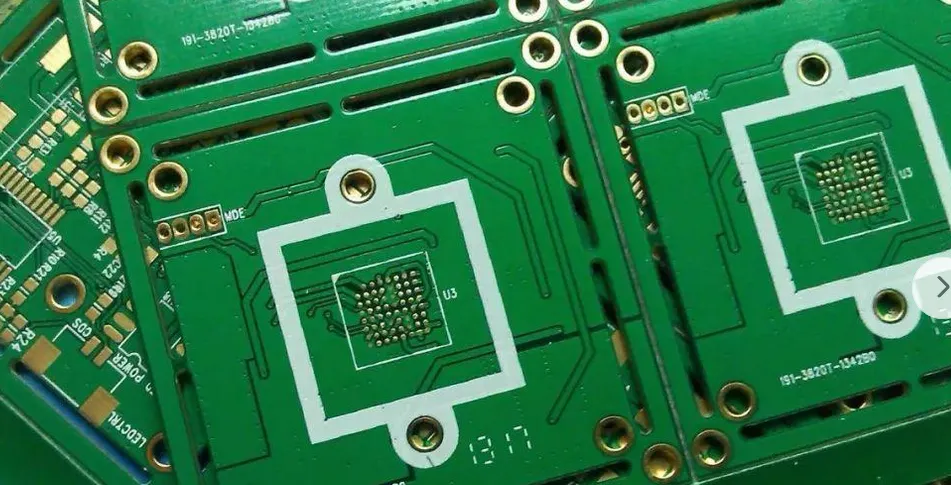
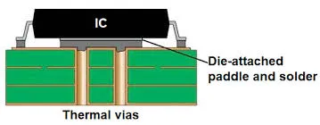
4. Overlooking Thermal Management
Thermal issues can cripple PCB performance, especially in high-power applications like LED lighting or motor controllers. A common mistake is placing heat-generating components, such as power MOSFETs, without adequate thermal reliefs or heatsinks. For example, a MOSFET dissipating 10 W without proper thermal vias can reach temperatures exceeding 150°C, risking component failure.
Another error is ignoring the thermal properties of the PCB material. Standard FR4 (Tg 130-140°C) may not withstand lead-free soldering temperatures (above 260°C) for high-Tg applications, leading to delamination.
How to Avoid It: Identify heat-generating components during the design phase and add thermal vias or heatsinks. Use PCB materials with higher Tg (e.g., 170°C) for lead-free processes. Simulate thermal performance with tools like ANSYS to ensure temperatures stay within safe limits (e.g., below 100°C for most components).
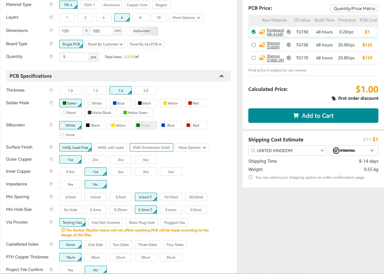
5. Choosing Inappropriate Materials
Selecting the wrong PCB material can lead to performance issues or increased costs. For instance, using standard FR4 for a high-frequency RF board (e.g., 2.4 GHz Wi-Fi) can cause signal loss due to its high dielectric constant (Er ~4.4). Materials like Rogers RO4350B (Er ~3.48) are better suited but cost more. Conversely, over-specifying exotic materials for low-frequency applications inflates costs unnecessarily.
A practical example: an engineer designing a 10-layer PCB for a server might choose FR4 without checking availability, only to discover their supplier doesn't stock it in the required thickness (e.g., 1.6 mm), causing delays.
How to Avoid It: Match the material to your application—FR4 for general-purpose boards, Rogers for RF, or metal-core for high-power designs. Check material availability and UL approval with your supplier during the design phase. Request a stack-up review to ensure compatibility with your layer count and performance needs.
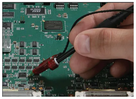
6. Neglecting Prototyping and Testing
Skipping prototyping to save time or costs is a risky move. Without a prototype, you can't verify functionality, signal integrity, or thermal performance before full production. For example, a PCB designed for a 1 GHz processor might work in simulation but fail in real-world testing due to EMI issues from poorly routed traces.
Prototyping also catches assembly issues, like misaligned footprints. A 0.1 mm mismatch between a QFN package and its landing pattern can prevent proper soldering, leading to a 30% failure rate in assembly.
How to Avoid It: Always order a small batch of prototypes (e.g., 5-10 boards) before full production. Test them using multimeters, oscilloscopes, or network analyzers to validate performance. Iterate on the design based on test results to eliminate errors.
7. Poor Communication with the Manufacturer
Miscommunication with your PCB manufacturer can derail your project. For instance, failing to specify lead-free soldering requirements might result in boards that can't withstand high-temperature reflow (260°C+), causing defects. Similarly, not clarifying panelization needs for odd-shaped boards can lead to costly custom SMT fixtures.
A case study: an engineer ordered 100 PCBs without discussing fiducial requirements, only to learn the manufacturer needed three fiducials per board for automated assembly, delaying production by a week.
How to Avoid It: Maintain open communication with your manufacturer from the start. Provide clear specifications for board material, soldering process, and panelization. Request a pre-production review to align expectations and catch potential issues.
How ALLPCB Supports Your PCB Ordering Success
At ALLPCB, we understand the challenges engineers face when ordering PCBs. Our quick-turn prototyping services deliver high-quality boards in as little as 24 hours, allowing you to test and iterate designs swiftly. With global logistics and advanced manufacturing capabilities, we ensure precise fabrication and assembly, even for complex, high-speed PCBs. Our team provides free DFM checks and stack-up reviews, helping you avoid costly mistakes like impedance mismatches or thermal issues. By partnering with ALLPCB, you gain a reliable ally to streamline your PCB ordering process and bring your designs to life efficiently.
Conclusion: Order PCBs with Confidence
Ordering PCBs is a complex process, but avoiding these common mistakes can make it smoother and more cost-effective. By prioritizing DFM checks, submitting complete files, addressing signal integrity, managing thermal issues, choosing the right materials, prototyping thoroughly, and communicating clearly with your manufacturer, you'll set your project up for success. Each step requires attention to detail, but the payoff is a reliable, high-performing PCB that meets your design goals.
Ready to order your next PCB? Take these lessons to heart, partner with a trusted manufacturer, and ensure your project moves from concept to reality without a hitch.