 ALLPCB


Are you facing issues like undercutting, over-etching, or uneven etching in your PCB manufacturing process? These common PCB etching problems can lead to defective boards, poor performance, and costly rework. In this comprehensive guide, we'll dive deep into the causes of these issues, including PCB undercutting causes and uneven etching in PCBs, and provide practical PCB over-etching solutions to help you troubleshoot and prevent defects. Whether you're a beginner or an experienced engineer, this post will equip you with the knowledge to achieve high-quality results in your PCB production.
What Is PCB Etching and Why Does It Matter?
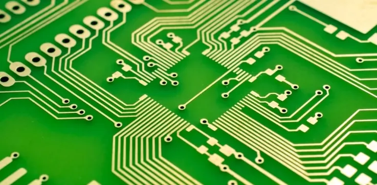
PCB etching is a critical step in the manufacturing of printed circuit boards. It involves removing unwanted copper from the board's surface to create the desired circuit patterns. This process uses a chemical solution, often an etchant like ferric chloride or ammonium persulfate, to dissolve the exposed copper while leaving the protected areas (covered by a resist layer) intact. The precision of etching directly impacts the board's electrical performance, signal integrity, and overall reliability.
When etching goes wrong, it can result in defects like undercutting, over-etching, or uneven etching, which compromise the board's functionality. For instance, undercutting can weaken traces, while over-etching might remove too much copper, leading to open circuits. Understanding and troubleshooting PCB defects early can save time, reduce waste, and ensure consistent quality in your projects.
Common PCB Etching Problems and Their Impact
Before diving into solutions, let's explore the most common PCB etching problems and how they affect your boards. These issues can disrupt signal transmission, cause electrical shorts, or even render a board unusable.
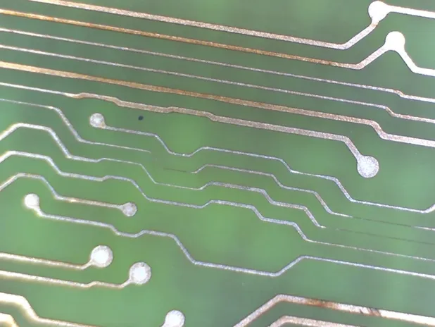
1. Undercutting in PCB Etching
Undercutting occurs when the etchant removes copper not only from the surface but also from underneath the edges of the resist layer. This results in traces that are narrower at the base than at the top, creating a trapezoidal or “undercut” shape. Severe undercutting can weaken traces, increasing the risk of breakage or poor conductivity. It often happens when the etching process is not well-controlled or when the resist layer is not properly adhered to the copper.
Impact: Undercutting can alter the impedance of traces, especially in high-frequency applications where trace width is critical. For example, a trace designed to have a 50-ohm impedance might deviate to 55 ohms or more due to reduced width, affecting signal integrity.
2. Over-Etching Issues
Over-etching happens when the etchant removes more copper than intended, often due to prolonged exposure to the chemical solution. This can lead to excessively thin traces, open circuits, or complete removal of small features like pads or vias. Over-etching is a common problem in both professional and DIY PCB production when timing or etchant concentration is not optimized.
Impact: Over-etched boards may fail electrical testing due to broken connections. In high-density designs, even a small deviation of 0.1 mm in trace width can disrupt the circuit's performance, especially for signals operating at speeds above 1 GHz.
3. Uneven Etching on PCBs
Uneven etching refers to inconsistent copper removal across the board's surface. Some areas may be over-etched while others remain under-etched, leading to irregular trace widths and poor circuit uniformity. This issue often stems from improper agitation, uneven resist application, or variations in etchant temperature.
Impact: Uneven etching can cause inconsistent electrical performance across the board. For instance, variations in trace thickness might lead to differing resistance values, affecting current distribution in power circuits.
Causes of PCB Etching Problems
Understanding the root causes of PCB etching problems is the first step in troubleshooting and preventing them. Below, we break down the primary reasons behind undercutting, over-etching, and uneven etching in PCBs.
PCB Undercutting Causes
- Poor Resist Adhesion: If the photoresist or etch mask does not adhere tightly to the copper, etchant can seep underneath, causing undercutting. This is often due to surface contamination or insufficient cleaning before resist application.
- Excessive Etching Time: Leaving the board in the etchant for too long allows the chemical to attack the sides of the traces, even under the resist layer.
- High Etchant Concentration: A highly concentrated etchant can react too aggressively, dissolving copper faster than intended and leading to undercutting.
- Inadequate Resist Thickness: A thin resist layer may break down during etching, exposing more copper to the etchant than planned.
Causes of Over-Etching in PCBs
- Prolonged Exposure: If the board remains in the etchant beyond the optimal time, even protected areas can start to erode, resulting in over-etching.
- Incorrect Etchant Temperature: Higher temperatures accelerate the etching process. For example, an etchant at 50°C might etch 30% faster than at 30°C, increasing the risk of over-etching if not monitored.
- Improper Etchant Mix: Using a solution with too high a concentration of active chemicals can cause rapid copper removal, leading to over-etched traces.
Reasons for Uneven Etching on PCBs
- Inconsistent Agitation: Without proper stirring or movement of the etchant, some areas of the board may receive more exposure than others, causing uneven copper removal.
- Uneven Resist Application: If the resist layer is applied inconsistently, certain areas may be less protected, leading to faster etching in those spots.
- Temperature Variations: Fluctuations in etchant temperature across the tank can result in different etching rates on the same board.
- Old or Depleted Etchant: Overused etchant loses its effectiveness, leading to slower etching in some areas and uneven results.
PCB Over-Etching Solutions and Troubleshooting Tips
Now that we've identified the causes of PCB etching problems, let's explore actionable solutions to address undercutting, over-etching, and uneven etching. These troubleshooting tips can help you achieve consistent, high-quality results in your PCB production.
Solutions for PCB Undercutting
- Optimize Etching Time: Monitor the etching process closely and remove the board as soon as the exposed copper is fully dissolved. For a standard 1 oz copper layer, etching might take 5-10 minutes at 40°C with a fresh etchant solution, but always test with a small sample first.
- Improve Resist Adhesion: Clean the copper surface thoroughly with isopropyl alcohol or a mild abrasive before applying the resist to remove oils and contaminants. Ensure the resist is cured or dried properly before etching.
- Use a Lower Etchant Concentration: Dilute the etchant according to manufacturer guidelines to slow down the reaction rate, reducing the chance of undercutting.
- Apply a Thicker Resist Layer: If using a photoresist, ensure it is applied evenly and at the recommended thickness (typically 1-2 mils) to prevent breakdown during etching.
Fixing Over-Etching Issues
- Control Etching Time Precisely: Use a timer and regularly inspect the board during etching. For a 1 oz copper layer, check every 2-3 minutes to avoid overexposure.
- Maintain Optimal Etchant Temperature: Keep the etchant solution at a stable temperature, ideally between 30-40°C, to ensure a consistent etching rate. Use a thermometer to monitor the solution during the process.
- Test Etchant Strength: Before full-scale etching, test the solution on a scrap piece of copper-clad board to determine the ideal exposure time and avoid over-etching.
- Use Fresh Etchant: Replace the etchant solution when it becomes saturated with dissolved copper, as old solutions can behave unpredictably and cause over-etching.
Addressing Uneven Etching on PCBs
- Ensure Proper Agitation: Use a pump, air bubbles, or manual stirring to keep the etchant moving evenly across the board. Consistent agitation prevents localized over-etching or under-etching.
- Apply Resist Uniformly: Whether using a spray, roller, or photoresist film, ensure the resist covers the copper evenly. Double-check for air bubbles or gaps before etching.
- Control Etchant Temperature: Use a heating element with a thermostat to maintain a uniform temperature throughout the etching tank, avoiding hot or cold spots.
- Refresh Etchant Regularly: Monitor the etchant’s condition and replace it after etching a certain number of boards (e.g., after 1-2 square feet of copper removal, depending on the solution's capacity).
Preventive Measures for Consistent PCB Etching
While troubleshooting PCB defects is essential, preventing etching problems in the first place is even better. Here are some best practices to ensure consistent results in your PCB etching process.
- Standardize Your Process: Document the etching parameters, including time, temperature, and etchant concentration, for every batch. Repeat these conditions to achieve uniformity across projects.
- Use High-Quality Materials: Invest in reliable resist materials and fresh etchant solutions to minimize variability in the etching process.
- Calibrate Equipment: Regularly check and calibrate any heating elements, timers, or agitation systems to ensure they operate within specified ranges.
- Train Personnel: Ensure that everyone involved in the etching process understands the importance of timing, safety, and proper handling of chemicals to avoid human error.
- Perform Test Runs: Before etching a full batch of boards, run a test on a small prototype to fine-tune your process and catch potential issues early.
Advanced Tips for High-Precision PCB Etching
For engineers working on high-density or high-frequency PCBs, precision in etching is even more critical. Here are advanced strategies to tackle complex PCB etching challenges.
- Use Spray Etching Systems: Spray etching, where etchant is sprayed onto the board under controlled pressure, can reduce undercutting by ensuring even exposure. This method is often used in professional settings for finer trace widths below 0.1 mm.
- Implement Etch Factor Compensation: During PCB design, account for the expected undercutting by slightly widening traces (e.g., by 0.05 mm) to compensate for material loss during etching.
- Monitor Etchant Chemistry: Use titration or chemical testing kits to measure the etchant's copper content and pH over time, adjusting or replacing the solution as needed to maintain consistent performance.
- Adopt Dry Film Photoresist: For finer details, dry film photoresist offers better adhesion and resolution compared to liquid resists, reducing the risk of undercutting or uneven etching.
Conclusion: Mastering PCB Etching for Quality Results
Troubleshooting PCB etching problems like undercutting, over-etching, and uneven etching is essential for producing reliable and high-performing printed circuit boards. By understanding the causes of these issues—such as poor resist adhesion, incorrect etching times, or inconsistent agitation—and applying the solutions outlined in this guide, you can significantly improve your etching process. Whether you're addressing PCB undercutting causes or seeking PCB over-etching solutions, the key lies in precision, consistency, and proactive prevention.
With the tips and strategies shared in this post, you're well-equipped to tackle common PCB etching challenges and achieve professional-grade results. Remember to standardize your process, use high-quality materials, and continuously monitor and adjust your setup for optimal performance. By mastering the art of etching, you'll ensure your PCBs meet the highest standards of quality and reliability for any application.Let's go start your PCB prototype at ALLPCB!


