 ALLPCB


Are you an electrical engineer looking to master the PCB etching process? Whether you're a seasoned professional or just starting out, understanding how to etch a printed circuit board (PCB) is crucial for creating reliable and efficient circuits. In this comprehensive guide, we’ll walk you through the PCB etching process steps, highlight the best PCB etching chemicals, provide a PCB etching troubleshooting guide, discuss PCB etching design considerations, and share essential PCB etching safety tips. Let’s dive into the details with ALLPCB to help you achieve perfect circuits every time!
What Is PCB Etching and Why Does It Matter?
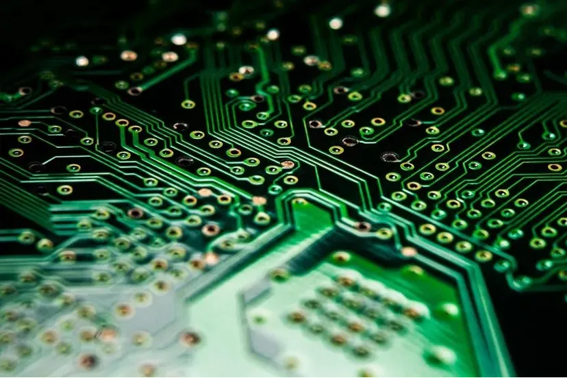
PCB etching is a critical step in the manufacturing of printed circuit boards. It involves removing unwanted copper from a copper-clad board to create the desired circuit pattern. This process directly impacts the performance and reliability of electronic devices, making it a skill every electrical engineer must master. A well-etched PCB ensures proper signal integrity, reduces noise, and prevents short circuits—key factors for high-quality electronics.
In the sections below, we’ll break down everything you need to know about PCB etching, from design to execution, with practical tips tailored for engineers. Let’s get started with the foundational steps.
PCB Etching Process Steps: A Step-by-Step Breakdown
Creating a flawless PCB starts with following a systematic etching process. Here’s a detailed guide to the PCB etching process steps to ensure precision and consistency in your work.
Step 1: Design Your PCB Layout
Before etching, you need a clear PCB design. Use PCB design software like Eagle, KiCad, or Altium Designer to create a layout of your circuit. Ensure the design accounts for trace widths (typically 0.2–0.5 mm for standard applications) and spacing to avoid signal interference. Export the design as a mirrored image for printing, as it will be transferred to the board.
Step 2: Transfer the Design to the Copper Board
Clean the copper-clad board with isopropyl alcohol to remove dirt and fingerprints. Then, transfer your design onto the board using one of these methods:
- Toner Transfer Method: Print the design on glossy paper using a laser printer and iron it onto the board. The heat transfers the toner, which acts as a resist during etching.
- Photoresist Method: Apply a photoresist film to the board, expose it to UV light through a printed transparency of your design, and develop it to reveal the copper pattern.
Both methods work well, but the photoresist method offers higher precision for complex designs with trace widths below 0.3 mm.
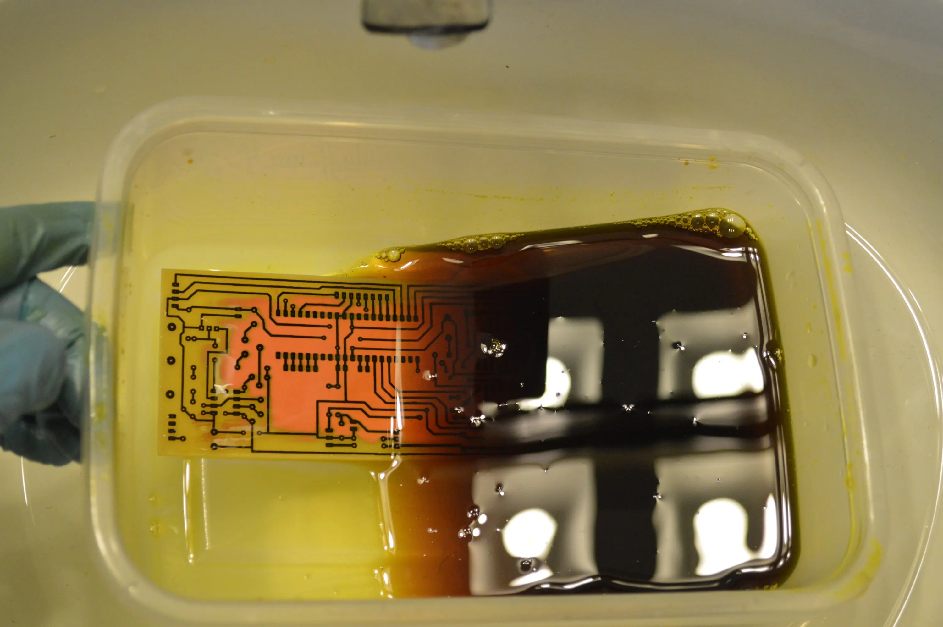
Step 3: Etch the Board
Immerse the board in an etching solution to remove unprotected copper. Common etchants include ferric chloride or cupric chloride (more on chemicals later). Agitate the solution gently to speed up the process, which typically takes 10–30 minutes depending on the copper thickness (e.g., 1 oz copper, or 35 μm, etches faster than 2 oz, or 70 μm). Monitor the board to avoid over-etching, which can damage fine traces.
Step 4: Clean and Inspect
Once etching is complete, rinse the board with water to stop the chemical reaction. Remove the resist layer using acetone or a resist stripper. Inspect the board under good lighting or with a magnifying glass to ensure all unwanted copper is gone and traces are intact. If issues are found, refer to the troubleshooting section below.
Step 5: Drill and Finish
Drill holes for through-hole components using PCB drill bits (common sizes range from 0.8 mm to 1.2 mm). Finally, apply a solder mask or protective coating to prevent oxidation and improve durability.
By following these steps meticulously, you can achieve clean, professional-grade PCBs for your projects. Now, let’s explore the chemicals that make this process possible.
Best PCB Etching Chemicals: Choosing the Right Solution
Selecting the right etchant is vital for efficient and safe PCB etching. Here, we’ll cover the best PCB etching chemicals used by engineers, along with their pros and cons.
1. Ferric Chloride (FeCl?)
Ferric chloride is the most popular etchant due to its affordability and effectiveness. It works by oxidizing copper into copper chloride, typically taking 10–20 minutes for 1 oz copper boards at room temperature (around 25°C).
- Pros: Widely available, cost-effective, reliable for hobbyists and small-scale production.
- Cons: Stains surfaces and clothing, slower etching time compared to alternatives, disposal requires careful handling due to environmental concerns.
2. Cupric Chloride (CuCl?)
Cupric chloride is a regenerable etchant, meaning it can be reused by adding hydrochloric acid and oxygen (via air bubbling). It etches faster than ferric chloride, often completing in 5–15 minutes.
- Pros: Faster etching, reusable with proper maintenance, less staining.
- Cons: More complex to prepare and maintain, requires additional equipment like an air pump.
3. Hydrogen Peroxide and Hydrochloric Acid Mix
This DIY etchant combines 3% hydrogen peroxide with muriatic acid (HCl). It’s a low-cost option that etches quickly, often in under 10 minutes for thin copper layers.
- Pros: Cheap and accessible, fast etching speed.
- Cons: Highly corrosive, produces toxic fumes, unstable shelf life.
For most engineers, ferric chloride strikes a balance between ease of use and effectiveness. However, if speed and reusability are priorities, consider cupric chloride for larger projects. Always prioritize safety when handling these chemicals—more on that later.

PCB Etching Design Considerations: Plan for Success
Before you start etching, thoughtful design can prevent many common issues. Here are key PCB etching design considerations to keep in mind.
Trace Width and Spacing
Ensure trace widths are appropriate for the current they’ll carry. For example, a 10 mA signal can use a 0.2 mm trace, while a 1 A power line may need 1.5–2 mm. Maintain at least 0.2 mm spacing between traces to prevent shorting during etching, especially for high-density designs.
Copper Thickness
Standard copper thickness is 1 oz (35 μm) or 2 oz (70 μm) per square foot. Thicker copper takes longer to etch and may require stronger or hotter etchants, increasing the risk of undercutting (etching beneath the resist). Choose thickness based on your project’s current and thermal requirements.
Pad and Via Sizes
Design pads and vias with enough copper area to withstand minor over-etching. For instance, a pad diameter of 1.5–2 times the drill hole size (e.g., 1.2 mm pad for a 0.8 mm hole) ensures durability during processing.
Ground Planes and Heat Dissipation
Incorporate ground planes to reduce noise and improve signal integrity, especially for high-frequency circuits above 10 MHz. Leave sufficient copper around heat-generating components to dissipate heat effectively.
By addressing these design factors, you’ll minimize etching errors and produce reliable PCBs tailored to your application.
PCB Etching Troubleshooting Guide: Solving Common Issues
Even with careful planning, etching problems can arise. This PCB etching troubleshooting guide will help you identify and fix common issues.
Problem 1: Incomplete Etching
Symptom: Some copper remains on the board after etching.
Cause: Weak or old etchant, insufficient agitation, or low temperature.
Solution: Use fresh etchant, heat the solution to 40–50°C for faster reaction, and agitate the board during etching to ensure even exposure.
Problem 2: Over-Etching
Symptom: Traces are too thin or broken.
Cause: Board left in etchant too long or resist layer was weak.
Solution: Monitor etching progress closely (check every 5 minutes), and use a high-quality resist method like photoresist for fine traces.
Problem 3: Undercutting
Symptom: Etchant eats beneath the resist, narrowing traces.
Cause: Etchant too strong or etching time too long.
Solution: Dilute the etchant slightly or reduce etching time. For ferric chloride, a 1:1 mix with water can slow the reaction for better control.
Problem 4: Resist Peeling Off
Symptom: Toner or photoresist lifts during etching, exposing unwanted copper.
Cause: Poor adhesion or contamination on the board.
Solution: Clean the board thoroughly before applying resist, and ensure proper heat or exposure during transfer.
By addressing these issues promptly, you can salvage a project and improve your technique for future PCBs.
PCB Etching Safety Tips: Protect Yourself and Your Workspace
Handling chemicals and tools during PCB etching poses risks. Follow these PCB etching safety tips to ensure a safe working environment.
1. Wear Protective Gear
Always wear chemical-resistant gloves, safety goggles, and a lab coat or apron when handling etchants like ferric chloride or hydrochloric acid. These chemicals can cause skin burns or eye damage on contact.
2. Work in a Ventilated Area
Etching chemicals can release harmful fumes, especially hydrogen peroxide and HCl mixtures. Use a fume hood or work outdoors to avoid inhaling toxic vapors. If indoors, ensure a fan or exhaust system is active.
3. Store and Dispose of Chemicals Properly
Keep etchants in labeled, sealed containers away from children and pets. Never pour used chemicals down the drain; neutralize them first (e.g., add baking soda to acidic solutions until pH is 7) and follow local hazardous waste disposal guidelines.
4. Avoid Skin and Surface Contact
Ferric chloride stains skin and surfaces. Use plastic or glass trays for etching, and cover your workspace with disposable sheets. If accidental contact occurs, rinse with plenty of water immediately.
5. Keep Emergency Supplies Handy
Have a first aid kit, eyewash solution, and baking soda (for neutralizing spills) nearby. Quick response to accidents can minimize injury.
Safety isn’t just a precaution—it’s a priority. Protect yourself to focus on creating great circuits without unnecessary risks.
Conclusion: Mastering PCB Etching for Perfect Circuits
PCB etching is both an art and a science, requiring careful planning, the right tools, and attention to detail. By following the PCB etching process steps, choosing the best PCB etching chemicals, considering critical PCB etching design considerations, using our PCB etching troubleshooting guide, and adhering to PCB etching safety tips, you can create high-quality circuits for any project. Whether you’re prototyping a new device or producing boards for a client, these practices will ensure success.


