 ALLPCB


If you're looking for a reliable and efficient way to test printed circuit boards (PCBs) during prototyping or low-volume production, flying probe testing is the answer. This method offers flexibility, precision, and cost-effectiveness, making it ideal for small batches and early-stage designs. In this comprehensive guide, we'll dive into what flying probe testing is, how it works, its benefits for PCB prototype testing and low-volume PCB test scenarios, the associated flying probe test cost, and how to access flying probe testing services. Let's explore why this needle probe testing approach is a game-changer for engineers and designers.
What Is Flying Probe PCB Testing?
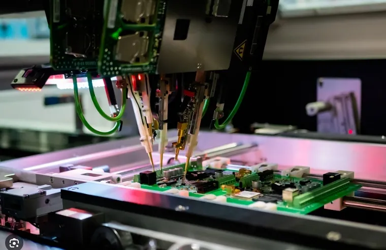
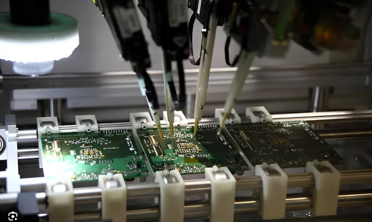
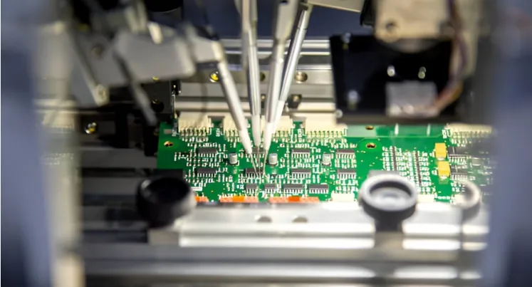
Flying probe testing is a modern, fixtureless method used to evaluate the electrical performance of PCBs. Unlike traditional in-circuit testing (ICT) that requires custom test fixtures, flying probe testing uses movable probes—often referred to as needle probes—to make contact with specific test points on the board. These probes "fly" across the PCB, following pre-programmed paths to check for issues like open circuits, short circuits, and component failures.
This technique is especially valuable for PCB prototype testing and low-volume PCB test needs because it eliminates the need for expensive fixtures. It’s a highly adaptable solution that can be quickly set up for different board designs, making it perfect for projects where designs are still evolving or production runs are small.
How Does Flying Probe Testing Work?
The flying probe testing process is straightforward yet highly precise. Here's a step-by-step breakdown of how it operates:
- Programming: Engineers upload the PCB design data, including test points and expected electrical values, into the flying probe testing system. This data guides the probes to the correct locations on the board.
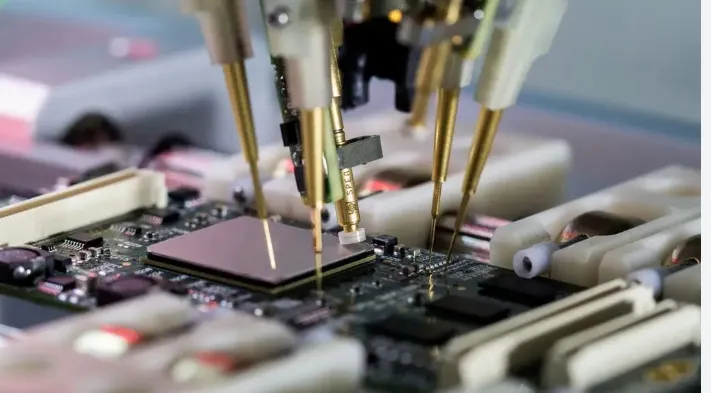
- Probe Movement: The system uses robotic arms to move the needle probes across the PCB. Typically, there are two to six probes, depending on the equipment, which work simultaneously to test multiple points.
- Electrical Testing: The probes measure parameters like resistance, capacitance, and continuity. For instance, they can detect if a circuit has a resistance value outside the acceptable range (e.g., above 10 ohms for a connection that should be near 0 ohms).
- Reporting: After testing, the system generates a detailed report highlighting any defects or anomalies, such as a short circuit between adjacent traces or an open connection at a solder joint.
This method is incredibly accurate, often achieving a test coverage of over 95% for most PCB designs. It’s also fast for small runs, with testing times ranging from a few minutes to an hour per board, depending on complexity.
Benefits of Flying Probe Testing for Prototypes and Low Volumes
Flying probe testing stands out as the go-to choice for engineers working on prototypes and low-volume production. Here are some key advantages that make it ideal for these scenarios:
1. No Need for Custom Fixtures
Traditional ICT requires a custom test fixture for each PCB design, which can cost thousands of dollars and take weeks to build. Flying probe testing, on the other hand, is fixtureless. This eliminates upfront costs and setup time, making it perfect for PCB prototype testing where designs may change frequently.
2. Quick Turnaround Time
Since there’s no fixture to design or build, flying probe testing can be set up in a matter of hours. For low-volume PCB test needs, this means faster feedback on design flaws, allowing engineers to iterate quickly. For example, a prototype batch of 10 boards can often be tested within a single day.
3. High Flexibility for Design Changes
Prototypes often undergo multiple revisions. With flying probe testing, updating the test program for a new design version is as simple as uploading the revised data. This adaptability is a major plus for projects in the early stages of development.
4. Cost-Effective for Small Batches
The flying probe test cost is significantly lower than ICT for small runs. While ICT fixtures can cost between $5,000 and $20,000 per design, flying probe testing operates on a per-board or per-test basis, often ranging from $50 to $500 per board depending on complexity and service provider. This makes it a budget-friendly option for low-volume PCB test requirements.
5. Precision with Needle Probe Testing
The needle probes used in this method are incredibly precise, capable of contacting test points as small as 0.2 mm in diameter. This level of accuracy ensures that even densely populated boards with fine-pitch components are tested thoroughly, reducing the risk of undetected defects.
Flying Probe Test Cost: What to Expect
One of the most common concerns for engineers is the flying probe test cost. While it varies based on factors like board complexity, test coverage, and the service provider, here are some general guidelines to help you budget:
- Basic Testing for Simple Boards: For a small, single-sided PCB with fewer test points (e.g., under 100 points), costs can start as low as $50 to $100 per board.
- Complex Designs: For double-sided or multilayer boards with high-density components and over 500 test points, expect costs to range from $200 to $500 per board.
- Volume Discounts: Some providers offer discounts for batches, even in low-volume scenarios. Testing 10 to 50 boards might reduce the per-board cost by 10-20%.
- Additional Services: If you require advanced testing (e.g., capacitance or inductance measurements beyond basic continuity), costs may increase by $50 to $150 per board.
Compared to the high upfront investment of ICT fixtures, flying probe testing remains a cost-effective choice for prototypes and small production runs. It’s worth noting that costs can also depend on the turnaround time—rush services for same-day testing may come with a premium.
To get an accurate estimate, it’s best to request a quote from a provider offering flying probe testing services. Many companies provide detailed pricing based on your specific PCB design files.
Applications of Flying Probe Testing in PCB Prototype Testing
Flying probe testing shines in scenarios where flexibility and precision are critical. Here are some common applications in PCB prototype testing:
- Early-Stage Prototypes: During the initial design phase, engineers need to validate concepts and identify issues like incorrect component placement or trace routing errors. Flying probe testing provides quick feedback without the hassle of fixtures.
- Design Validation: Before moving to full-scale production, prototypes must meet strict electrical performance standards. Flying probe testing can verify parameters like signal integrity, ensuring that impedance values fall within acceptable ranges (e.g., 50 ohms for high-speed signals).
- Small Batch Testing: For pilot runs or limited-edition products, flying probe testing ensures quality without the expense of traditional testing methods.
This method is particularly useful for industries like IoT, medical devices, and automotive electronics, where prototypes often involve complex, high-density boards that require meticulous testing.
Choosing the Right Flying Probe Testing Services
Finding reliable flying probe testing services is crucial to ensuring the quality of your PCBs. Here are some tips to help you select the right provider for your low-volume PCB test or prototype needs:
- Experience and Expertise: Look for a provider with a proven track record in testing PCBs for your industry. Experienced providers are more likely to handle complex designs and provide actionable insights from test results.
- Equipment Capabilities: Ensure the provider uses modern flying probe testers with multiple probes (e.g., 4 or 6 probes) for faster and more comprehensive testing. Advanced systems can test boards with dimensions up to 24 x 20 inches and handle fine-pitch components.
- Turnaround Time: For prototype testing, speed is often critical. Choose a service that offers quick setup and testing, ideally within 24-48 hours for small batches.
- Cost Transparency: Opt for a provider that offers clear pricing without hidden fees. Request a detailed quote based on your PCB design to avoid surprises.
- Support and Reporting: A good service provider will offer detailed test reports and support to help you interpret results and address any issues. Look for providers that include visual defect mapping or failure analysis in their reports.
At ALLPCB, we understand the importance of reliable testing for your projects. Our flying probe testing services are designed to deliver precision and efficiency, ensuring your prototypes and low-volume batches meet the highest quality standards.
Limitations of Flying Probe Testing
While flying probe testing is an excellent choice for many scenarios, it’s important to be aware of its limitations:
- Not Ideal for High-Volume Production: For large-scale runs (e.g., thousands of boards), the per-board testing time of flying probe systems can be slower than ICT with fixtures. In such cases, the upfront cost of a fixture may be justified.
- Limited Test Speed: Testing a single board with hundreds of test points can take several minutes, whereas ICT can test a board in seconds once the fixture is ready.
- Component Limitations: Some components, like those requiring functional testing under power, may not be fully evaluated with standard flying probe systems unless additional equipment is used.
Understanding these constraints can help you decide if flying probe testing is the right fit for your project or if a hybrid approach with other testing methods is needed.
Comparing Flying Probe Testing to Other Methods
To better appreciate the value of flying probe testing, let’s compare it to other common PCB testing methods:
- Flying Probe vs. In-Circuit Testing (ICT): ICT is faster for high-volume production but requires costly fixtures. Flying probe testing is slower per board but far more cost-effective for prototypes and low-volume runs due to its fixtureless nature.
- Flying Probe vs. Functional Testing: Functional testing evaluates a PCB under real-world operating conditions, which flying probe testing cannot fully replicate. However, flying probe testing excels at detecting manufacturing defects like shorts and opens.
- Flying Probe vs. Automated Optical Inspection (AOI): AOI focuses on visual defects like solder joint issues, while flying probe testing checks electrical performance. Combining both methods often provides the most comprehensive quality assurance.
For engineers working on small batches, flying probe testing often strikes the perfect balance between cost, speed, and accuracy.
Image Placement Suggestion: Place a comparison chart here showing flying probe testing vs. ICT and other methods in terms of cost, speed, and application. ALT Text: "Comparison chart of flying probe testing vs. other PCB testing methods."
Conclusion: Why Choose Flying Probe Testing?
Flying probe testing is a powerful, agile solution for PCB prototype testing and low-volume PCB test needs. Its fixtureless design, quick setup, and precision with needle probe testing make it an ideal choice for engineers looking to validate designs without breaking the budget. While the flying probe test cost varies based on complexity and provider, it remains a cost-effective option compared to traditional methods for small runs. By partnering with reliable flying probe testing services, you can ensure your boards meet quality standards and perform as expected.
Whether you're iterating on a new design or producing a limited batch of PCBs, flying probe testing offers the flexibility and accuracy needed to bring your projects to life. At ALLPCB, we’re committed to supporting your success with cutting-edge testing solutions tailored to your unique requirements. Embrace the agility of flying probe testing and take your PCB development to the next level.


