 ALLPCB


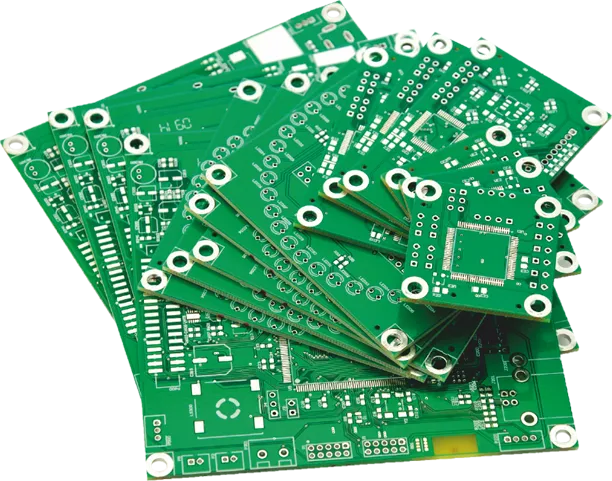
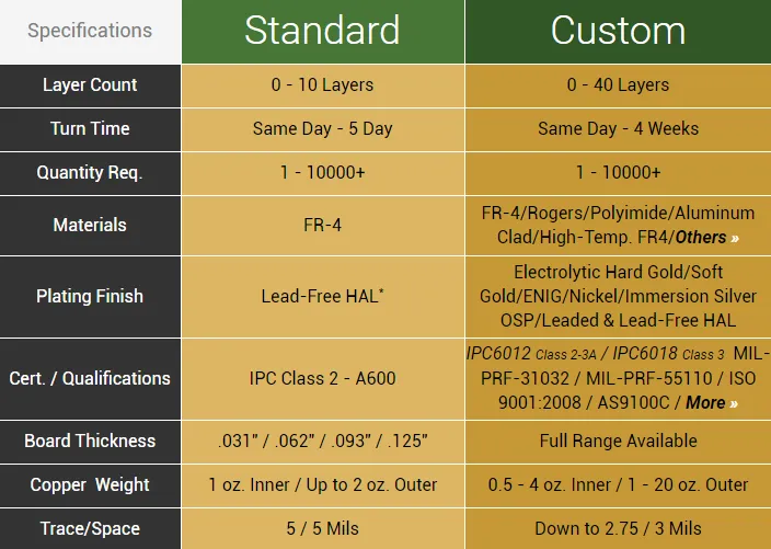
When it comes to optimizing project performance, custom PCBs (Printed Circuit Boards) often outshine standard sizes. The ability to tailor every aspect of the board—from layout to routing and signal impedance—ensures that your design meets specific requirements for speed, reliability, and efficiency. Unlike standard sizes, which are constrained by predefined dimensions and configurations, custom PCBs offer the flexibility to address unique challenges in board performance optimization. In this blog, we’ll dive deep into why custom PCBs are the better choice for enhancing project outcomes, focusing on layout precision, routing efficiency, and signal impedance control.
What Makes Custom PCBs a Game-Changer for Performance?
Custom PCBs are designed from the ground up to fit the exact needs of a project. Whether you're working on a compact IoT device or a high-speed communication system, a tailored board can significantly improve functionality. Standard sizes, while convenient and often cheaper, are built for general use and may not align with the specific demands of your application. This mismatch can lead to inefficiencies in power delivery, signal delays, or even electromagnetic interference (EMI). Custom PCBs eliminate these risks by allowing full control over every design element, ensuring optimal performance.
Board Performance Optimization: Tailoring for Success
One of the primary reasons custom PCBs excel is their potential for board performance optimization. Performance isn’t just about speed; it’s about reliability, power efficiency, and thermal management. With a custom design, you can prioritize the factors that matter most to your project. For instance, in a high-frequency application, you might need to minimize signal loss by using specific materials with low dielectric constants (e.g., a Dk value of 3.5 or lower). Standard boards often use generic materials like FR-4, which may not meet such precise needs and can result in signal degradation at frequencies above 1 GHz.
Moreover, custom PCBs allow you to optimize the board’s size and shape to fit within unique enclosures or space constraints. This can reduce unnecessary material costs and prevent issues like overheating due to poor component spacing. In contrast, standard sizes might force you to compromise on placement, leading to longer traces and higher resistance—both of which can degrade performance. By focusing on board performance optimization, custom designs ensure that every element works in harmony to deliver the desired results.
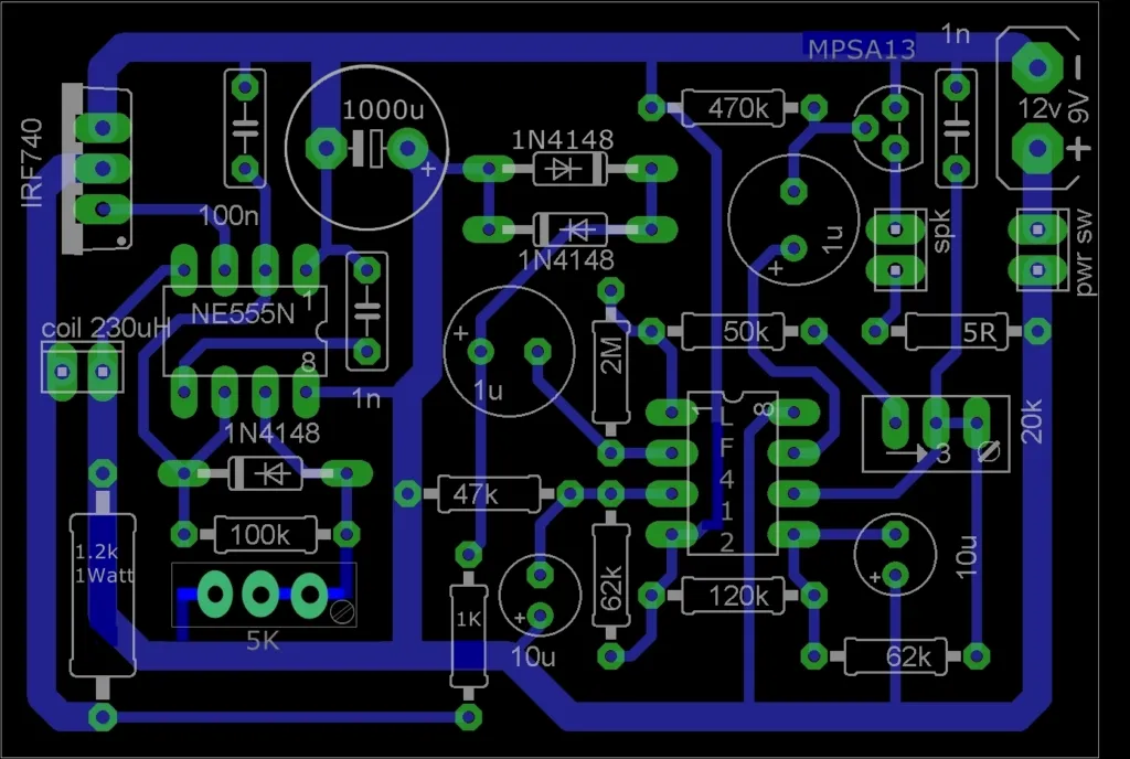
Layout Precision: Designing for Efficiency
The layout of a PCB plays a critical role in determining how well a circuit functions. Custom PCBs give you the freedom to create a layout that minimizes noise, reduces crosstalk, and ensures efficient power distribution. For example, in a high-speed digital circuit, placing critical components closer together on a custom board can shorten trace lengths, reducing latency and power loss. Studies show that reducing trace length by just 10% can decrease signal delay by up to 50 picoseconds in high-speed designs.
Standard-sized boards often come with predefined layouts or grid patterns that may not align with your component needs. This can lead to inefficient use of space, forcing longer traces or awkward component placement. Such compromises can introduce parasitic capacitance or inductance, which disrupts signal integrity. With a custom PCB, you can strategically position components to avoid these issues, ensuring a cleaner and more efficient layout. This level of precision is especially crucial for applications like RF circuits, where even a small deviation in layout can cause significant performance drops.
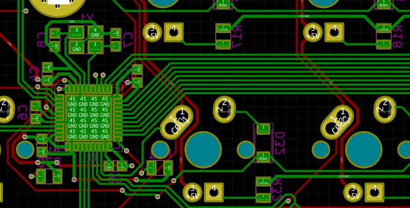
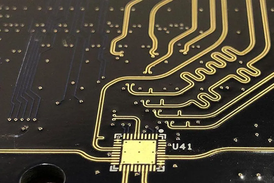
Routing Efficiency: Streamlining Signal Paths
Routing, or the process of connecting components with conductive traces, is another area where custom PCBs shine. Efficient routing is essential for minimizing signal delays, reducing EMI, and ensuring stable power delivery. Custom designs allow you to define trace widths, spacing, and paths based on the specific current and voltage requirements of your project. For instance, high-current traces might need a width of 50 mils or more to handle loads without overheating, while signal traces for a 5G application might require precise spacing to prevent crosstalk.
On standard-sized boards, routing options are often limited by the board’s fixed dimensions and pre-set via placements. This can result in longer, more convoluted traces that increase resistance and signal loss. In high-speed designs, longer traces can also cause timing issues, where signals arrive at different times, leading to data errors. Custom PCBs let you create direct, optimized routing paths, often incorporating techniques like differential pair routing for high-speed signals. This ensures that signals travel with minimal interference, boosting overall board performance.
Signal Impedance Control: Ensuring Signal Integrity
Signal impedance is a critical factor in maintaining signal integrity, especially in high-frequency and high-speed applications. Impedance mismatches can cause signal reflections, leading to data loss or corruption. Custom PCBs allow precise control over impedance by adjusting trace width, spacing, and the dielectric properties of the board material. For example, a 50-ohm impedance is standard for many RF applications, and achieving this requires exact trace dimensions (often calculated using tools based on the board’s stack-up and material properties).
Standard boards typically lack the flexibility to fine-tune impedance because their materials and layer configurations are fixed. This can be a significant drawback for projects where signal impedance must be tightly controlled, such as in telecommunications or automotive radar systems. With a custom PCB, you can specify materials with specific dielectric constants and design the stack-up to match your impedance targets. This level of control reduces signal reflections and ensures that data is transmitted accurately, even at speeds exceeding 10 Gbps.
Thermal Management: Preventing Overheating Issues
Heat dissipation is a common challenge in electronic designs, and custom PCBs offer superior solutions for thermal management. Overheating can degrade component performance and shorten the lifespan of a device. With a custom board, you can integrate thermal vias, heat sinks, and copper pours to direct heat away from sensitive areas. For instance, placing thermal vias under a high-power IC can reduce its operating temperature by up to 20°C, significantly improving reliability.
Standard-sized boards often lack the space or design flexibility to implement advanced thermal solutions. Components might be crowded together, or there may not be enough room for proper heat dissipation structures. This can lead to hot spots that cause system failures. Custom PCBs allow you to space out heat-generating components and design the board with thermal performance in mind, ensuring stable operation even under heavy loads.
Cost vs. Value: Are Custom PCBs Worth the Investment?
One concern with custom PCBs is the initial cost, as they are typically more expensive to design and manufacture than standard sizes. However, the long-term value often outweighs this upfront investment. By optimizing layout, routing, and signal impedance, custom boards reduce the risk of performance issues that could lead to costly redesigns or product failures. Additionally, they can lower production costs by minimizing material waste and ensuring efficient assembly processes.
For small-scale or prototype projects, the cost difference might seem significant. But for high-volume production or mission-critical applications, the improved performance and reliability of custom PCBs can save money in the long run. They also enable faster time-to-market by reducing the need for iterative fixes, which is invaluable in competitive industries.
Applications Where Custom PCBs Make a Difference
Custom PCBs are particularly beneficial in specific industries and applications where performance is non-negotiable. In aerospace, for example, boards must withstand extreme conditions while maintaining signal integrity for navigation systems. Custom designs allow for rugged materials and precise layouts to meet these demands. Similarly, in medical devices like pacemakers, compact custom boards ensure reliability in a confined space, where standard sizes might not fit.
In the realm of consumer electronics, custom PCBs enable sleeker, more efficient designs for smartphones and wearables. High-speed communication systems, such as 5G infrastructure, also rely on custom boards to manage signal impedance and routing for ultra-fast data transfer. These examples highlight how tailored designs address unique challenges that standard boards simply cannot handle.
How to Get Started with Custom PCB Design
Designing a custom PCB may seem daunting, but modern tools and services make the process accessible. Start by defining your project’s requirements, including size constraints, performance goals, and environmental factors. Use simulation software to test your layout and routing for issues like signal impedance mismatches or thermal hotspots. Collaborating with experienced manufacturing partners can also streamline the process, ensuring that your design is both feasible and optimized for production.
Pay attention to details like layer stack-up, material selection, and trace geometry during the design phase. These elements directly impact board performance optimization and can make or break your project. By investing time in planning, you’ll create a custom PCB that delivers exceptional results tailored to your needs.
Conclusion: Elevate Your Project with Custom PCBs
Custom PCBs offer unparalleled advantages over standard sizes when it comes to project performance. From board performance optimization to precise layout and routing, they provide the flexibility to address specific challenges in your design. Signal impedance control ensures data integrity in high-speed applications, while tailored thermal management prevents overheating. Though the initial cost may be higher, the long-term benefits of reliability, efficiency, and reduced redesigns make custom PCBs a smart investment.
Whether you’re working on a cutting-edge tech product or a critical industrial system, custom PCBs empower you to push the boundaries of what’s possible. By focusing on the unique needs of your project, you can achieve superior performance that standard sizes simply can’t match. Embrace the power of customization and take your designs to the next level with a PCB built for success.


