 ALLPCB


If you're looking to optimize your PCB design for better performance and reduced electromagnetic interference (EMI), understanding PCB signal layer stackup is the key. A well-designed stackup, with proper signal layer order, EMI reduction in signal layers, signal layer impedance control, and reference plane proximity, ensures high-speed signals travel smoothly while minimizing noise. In this comprehensive guide, we'll uncover the secrets to crafting an effective stackup that boosts performance and keeps EMI in check.
What Is PCB Signal Layer Stackup and Why Does It Matter?
A PCB signal layer stackup refers to the arrangement of conductive layers, including signal layers and reference planes (like ground and power planes), within a printed circuit board. This structure dictates how signals propagate, how much interference they encounter, and how well the board manages power distribution. A poorly designed stackup can lead to signal degradation, crosstalk, and excessive EMI, which can cause system failures or compliance issues.
For modern high-speed designs, where signal speeds can exceed 1 GHz, a proper stackup is critical. It ensures signal integrity by controlling impedance, reduces EMI by providing clean return paths, and improves overall board reliability. Whether you're working on a 4-layer board for a simple device or a 12-layer board for complex electronics, mastering stackup design is essential.
The Basics of Signal Layer Order for Optimal Performance
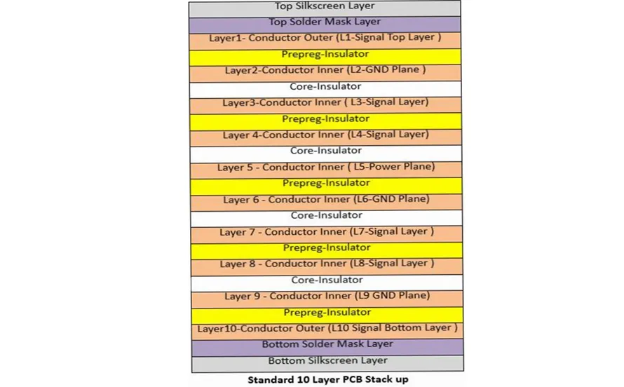
The order of signal layers in your PCB stackup directly impacts signal quality and EMI. The primary goal is to place high-speed signal layers close to their reference planes (ground or power) to maintain consistent impedance and provide a low-inductance return path for signals. Here's how to approach signal layer order:
- Top and Bottom Layers: Use these for low-speed signals or components. High-speed signals on outer layers are more prone to EMI radiation since they lack an adjacent reference plane on one side.
- Inner Layers: Place high-speed signals on inner layers, sandwiched between reference planes. For a 4-layer board, a common stackup is Signal-Ground-Power-Signal, ensuring each signal layer is next to a reference plane.
- Layer Grouping: Group related signals (like differential pairs) on the same layer to minimize skew and maintain timing integrity.
For example, in a 6-layer PCB, a typical stackup might be Signal-Ground-Signal-Signal-Power-Signal. This ensures that each signal layer has a nearby reference plane, reducing loop inductance and EMI. Studies show that improper layer ordering can increase crosstalk by up to 30% in high-speed designs, so planning your stackup early is crucial.
EMI Reduction in Signal Layers: Key Strategies
Electromagnetic interference (EMI) can disrupt signal integrity and cause your design to fail regulatory tests. Effective EMI reduction in signal layers starts with a thoughtful stackup design. Here are proven strategies to minimize EMI:
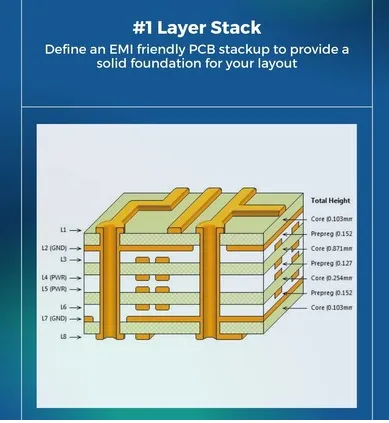
- Use Continuous Reference Planes: Ensure ground and power planes are unbroken beneath signal layers. Gaps or splits in reference planes can force return currents to take longer paths, creating larger loops that radiate EMI. A solid ground plane can reduce radiated emissions by up to 20 dB in some cases.
- Minimize Signal Layer Spacing: Keep signal layers close to their reference planes. A spacing of 5 mils between a signal layer and its reference plane is often ideal for high-speed designs, as it reduces loop area and EMI.
- Avoid Routing Over Plane Splits: Routing high-speed signals over splits in ground or power planes can lead to impedance discontinuities and increased EMI. Always route signals parallel to plane edges if splits are unavoidable.
- Use Guard Traces: For critical signals, add guard traces connected to ground on either side to shield against crosstalk and EMI. This is especially useful for analog signals in mixed-signal designs.
Signal Layer Impedance Control: Achieving Consistency
Impedance mismatches in high-speed designs can cause signal reflections, leading to data errors and degraded performance. Signal layer impedance control is about designing your stackup to maintain a consistent characteristic impedance (often 50 ohms for single-ended signals or 100 ohms for differential pairs). Here's how to achieve it:
- Layer Thickness and Dielectric Constant: The distance between a signal layer and its reference plane, along with the dielectric constant (Dk) of the material, determines impedance. For instance, a 50-ohm trace on a 4-layer board with FR-4 material (Dk ≈ 4.2) typically requires a trace width of 6-8 mils and a separation of 5 mils from the ground plane.
- Trace Width and Spacing: Use impedance calculators or simulation tools to determine the correct trace width and spacing for your target impedance. Narrower traces increase impedance, while wider traces decrease it.
- Reference Plane Continuity: Ensure the reference plane beneath a signal trace is continuous. Any interruption can alter the impedance, causing reflections. For example, a via transition without a nearby return via can increase impedance by 10-15% locally.
Maintaining impedance control is especially critical for high-speed interfaces like USB, HDMI, or PCIe, where signal integrity directly impacts data rates. A deviation of just 10% in impedance can lead to significant signal loss at frequencies above 1 GHz.
Reference Plane Proximity: Why It’s Critical
The concept of reference plane proximity ties directly into both impedance control and EMI reduction. The closer a signal layer is to its reference plane, the tighter the coupling, which results in lower loop inductance and better signal integrity. Here's why proximity matters:
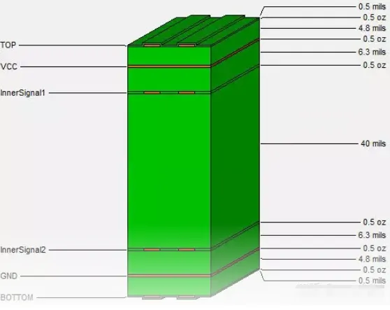
- Reduced Loop Area: A smaller distance between the signal layer and reference plane minimizes the loop area for return currents, reducing EMI radiation. For high-speed signals, aim for a separation of 3-5 mils in standard designs.
- Better Impedance Stability: Closer proximity ensures more consistent impedance, as the electric field between the signal trace and reference plane is stronger and less influenced by external factors.
- Improved Power Integrity: Close reference planes also help with power distribution by reducing noise on power rails, which can otherwise couple into signal layers.
In practice, for a 4-layer board, you might have a stackup with 5 mils between the top signal layer and the ground plane, 30 mils between ground and power, and another 5 mils between power and the bottom signal layer. This asymmetry prioritizes signal integrity on outer layers by keeping reference planes close. However, for more layers (like 8 or 10), balance becomes key to avoid excessive board thickness.
Common PCB Stackup Configurations for Different Layer Counts
Choosing the right stackup depends on your board's layer count and design requirements. Below are common configurations for various layer counts, optimized for signal integrity and EMI reduction:
4-Layer Stackup
- Layer 1: Signal (Low-Speed)
- Layer 2: Ground
- Layer 3: Power
- Layer 4: Signal (Low-Speed)
This setup is ideal for cost-effective designs, with ground and power planes providing reference for outer signal layers. High-speed signals should be avoided on outer layers if possible.
6-Layer Stackup
- Layer 1: Signal (Low-Speed)
- Layer 2: Ground
- Layer 3: Signal (High-Speed)
- Layer 4: Signal (High-Speed)
- Layer 5: Power
- Layer 6: Signal (Low-Speed)
This configuration allows high-speed signals on inner layers with adjacent reference planes, improving EMI performance.
8-Layer Stackup
- Layer 1: Signal (Low-Speed)
- Layer 2: Ground
- Layer 3: Signal (High-Speed)
- Layer 4: Power
- Layer 5: Ground
- Layer 6: Signal (High-Speed)
- Layer 7: Power
- Layer 8: Signal (Low-Speed)
Multiple ground and power planes provide excellent shielding and reference for high-speed signals, ideal for complex designs.
Practical Tips for Designing Your PCB Signal Layer Stackup
Now that we've covered the core principles, here are actionable tips to apply when designing your PCB signal layer stackup:
- Plan Early: Define your stackup before routing. Changing layer order mid-design can disrupt impedance and EMI planning.
- Use Simulation Tools: Leverage software to simulate signal integrity and EMI performance for your stackup. This helps catch issues before fabrication.
- Consult Material Data: Work with your PCB manufacturer to select materials with suitable dielectric constants (Dk) and loss tangents for your frequency range.
- Test and Iterate: After prototyping, measure signal integrity and EMI performance using oscilloscopes or network analyzers to validate your stackup design.
Conclusion: Master Your Stackup for Superior PCB Performance
Crafting an optimized PCB signal layer stackup is both an art and a science. By carefully planning your signal layer order, focusing on EMI reduction in signal layers, ensuring signal layer impedance control, and maintaining reference plane proximity, you can achieve exceptional performance and reliability in your designs. Whether you're working on a simple 4-layer board or a complex multi-layer system, these principles will guide you to success.
Start with a clear understanding of your design requirements, choose the right stackup configuration, and pay attention to the smallest details like layer spacing and plane continuity. With these secrets in hand, your PCBs will not only perform better but also pass EMI compliance tests with ease, saving you time and resources in the long run.





