 ALLPCB


In the fast-evolving world of artificial intelligence (AI), AI accelerator PCBs (Printed Circuit Boards) are at the heart of high-performance computing systems. These specialized boards power machine learning algorithms, neural networks, and data processing tasks. However, designing PCBs for AI accelerators comes with significant challenges, especially when it comes to maintaining signal integrity. Issues like crosstalk, signal reflection, impedance mismatches, and high-speed routing problems can degrade performance and cause system failures. So, how can engineers overcome these hurdles? In this blog, we’ll explore the key signal integrity challenges in AI accelerator PCB design and provide practical mitigation techniques for high-speed routing, impedance control, crosstalk reduction, and signal reflection management.
Whether you’re an engineer working on cutting-edge AI hardware or a designer looking to optimize your PCB layouts, this guide will walk you through actionable solutions to ensure your designs meet the demands of modern AI applications. Let’s dive into the details of AI accelerator PCB signal integrity and uncover strategies to tackle these complex issues.
What is Signal Integrity in AI Accelerator PCB Design?
Signal integrity refers to the quality of an electrical signal as it travels through a PCB. In AI accelerator PCBs, where data rates often exceed 10 Gbps and frequencies climb into the multi-GHz range, maintaining signal integrity is critical. Poor signal integrity can lead to data errors, timing issues, and reduced system reliability—problems that AI systems, which rely on massive parallel processing and real-time computations, cannot afford.
The primary challenges in maintaining AI accelerator PCB signal integrity include managing high-speed signal routing, controlling impedance, reducing crosstalk, and minimizing signal reflections. These issues arise due to the dense layouts, high pin counts, and extreme operating conditions of AI hardware. In the following sections, we’ll break down each challenge and provide proven mitigation techniques to help you design robust PCBs for AI accelerators.

Challenge 1: High-Speed Routing in AI Accelerator PCBs
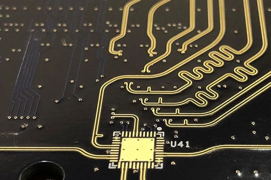
AI accelerators demand high-speed data transmission to handle massive datasets and complex computations. As signal speeds increase, the risk of signal degradation due to trace length mismatches, improper routing, and electromagnetic interference (EMI) also rises. High-speed routing AI PCB design must account for these factors to ensure signals arrive at their destination without distortion or delay.
Mitigation Techniques for High-Speed Routing
- Minimize Trace Lengths: Keep high-speed signal traces as short as possible to reduce propagation delays and signal loss. For instance, in designs operating at 25 Gbps, even a 1-inch difference in trace length can cause significant timing skew.
- Use Differential Pairs: Route high-speed signals as differential pairs to cancel out noise and improve signal integrity. Ensure consistent spacing (typically 5-10 mils) between the pair to maintain coupling.
- Avoid Sharp Corners: Use 45-degree bends or curved traces instead of 90-degree corners to prevent signal reflections and EMI. Sharp corners can act as antennas, radiating unwanted noise.
- Layer Stacking: Place high-speed traces on inner layers sandwiched between ground planes to shield them from external interference. A typical stack-up for AI PCBs might include 8-12 layers with dedicated ground and power planes.
By implementing these strategies, engineers can optimize high-speed routing AI PCB designs, ensuring clean signal transmission even at multi-Gbps speeds.
Challenge 2: Impedance Control in AI Accelerator PCBs
Impedance mismatches are a common cause of signal integrity issues in AI accelerator designs. When the impedance of a trace doesn’t match the source or load impedance, it causes signal reflections, leading to data errors. For AI systems operating at frequencies above 10 GHz, even a small mismatch (e.g., 5 ohms) can significantly degrade performance. Impedance control AI PCB design is essential to prevent these issues.
Mitigation Techniques for Impedance Control
- Calculate Trace Impedance: Use PCB design tools to calculate the characteristic impedance of traces based on their width, thickness, and dielectric material. For high-speed signals, a common target impedance is 50 ohms for single-ended traces and 100 ohms for differential pairs.
- Consistent Trace Width: Maintain uniform trace widths along the entire signal path to avoid impedance discontinuities. For example, a trace width of 5 mils might be used for a 50-ohm impedance on a standard FR-4 substrate with a dielectric constant of 4.2.
- Dielectric Material Selection: Choose low-loss dielectric materials with stable dielectric constants (e.g., Rogers or Isola materials) to maintain consistent impedance at high frequencies.
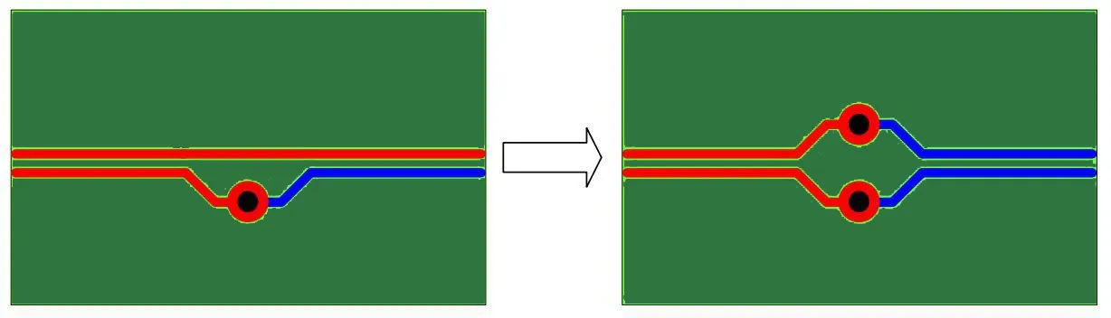
- Via Design: Minimize the use of vias in high-speed signal paths, as they can introduce impedance mismatches. When vias are unavoidable, use back-drilling to remove unused via stubs, reducing parasitic capacitance.
Proper impedance control AI PCB practices ensure that signals travel without unwanted reflections, preserving data integrity in AI accelerator systems.
Challenge 3: Crosstalk in AI Accelerator PCBs
Crosstalk occurs when a signal on one trace interferes with a neighboring trace, causing noise and potential data corruption. In AI accelerator PCBs, where traces are densely packed to accommodate high pin-count chips, crosstalk is a major concern. Crosstalk reduction AI PCB techniques are vital to maintain clean signal transmission.
Mitigation Techniques for Crosstalk Reduction
- Increase Trace Spacing: Maintain adequate spacing between adjacent traces to reduce capacitive and inductive coupling. A general rule of thumb is to keep spacing at least three times the trace width (e.g., 15 mils for a 5-mil trace).
- Use Ground Planes: Place continuous ground planes adjacent to signal layers to provide a return path for currents and shield traces from crosstalk. Ensure ground planes are unbroken under high-speed signals.
- Route Signals Orthogonally: On adjacent layers, route signals perpendicular to each other to minimize coupling. For example, if layer 2 has horizontal traces, layer 3 should have vertical traces.
- Guard Traces: Add grounded guard traces between high-speed signals to act as a barrier against crosstalk. Connect these traces to ground at multiple points for maximum effectiveness.
Implementing these crosstalk reduction AI PCB methods can significantly lower noise levels, ensuring reliable operation of AI accelerators even in dense layouts.
Challenge 4: Signal Reflection in AI Accelerator PCBs
Signal reflection happens when a signal encounters an impedance discontinuity, bouncing back along the trace and interfering with the original signal. In AI accelerator designs, where signals operate at high frequencies, reflections can cause ringing, overshoot, and data errors. Addressing signal reflection AI PCB issues is crucial for maintaining signal integrity.
Mitigation Techniques for Signal Reflection
- Termination Resistors: Use termination resistors at the end of high-speed traces to match the load impedance and absorb reflected signals. For a 50-ohm trace, a 50-ohm resistor placed near the receiver can prevent reflections.
- Avoid Stubs: Eliminate unused trace stubs, which act as antennas for reflected signals. If stubs are unavoidable, keep them shorter than 1/10th of the signal wavelength (e.g., less than 0.6 inches for a 10 GHz signal).
- Smooth Transitions: Ensure smooth transitions between different trace widths or layers to avoid sudden impedance changes. Gradual tapering of traces can help maintain signal continuity.
- Simulation Tools: Use signal integrity simulation software to model and predict reflection behavior before manufacturing. These tools can identify potential issues in the design phase, saving time and cost.
By applying these signal reflection AI PCB mitigation strategies, designers can prevent signal distortions and ensure reliable data transmission in AI systems.
Additional Best Practices for AI Accelerator PCB Signal Integrity
Beyond the specific challenges and techniques discussed, there are general best practices that can further enhance AI accelerator PCB signal integrity. These include:
- Power Delivery Network (PDN) Design: Ensure a low-impedance power delivery network with proper decoupling capacitors (e.g., 0.1 μF and 1 μF caps near ICs) to minimize power supply noise, which can affect signal quality.
- Thermal Management: AI accelerators generate significant heat, which can alter material properties and affect signal integrity. Use thermal vias and heat sinks to manage temperature and maintain consistent performance.
- Pre-Layout Simulation: Perform simulations during the design phase to identify potential signal integrity issues. Tools for electromagnetic analysis can predict crosstalk, reflections, and impedance mismatches before the board is built.
These practices, combined with the specific mitigation techniques for routing, impedance, crosstalk, and reflections, create a comprehensive approach to designing high-performance AI accelerator PCBs.
Conclusion: Building Reliable AI Accelerator PCBs
Designing PCBs for AI accelerators is no small feat. The combination of high-speed data rates, dense layouts, and extreme performance requirements makes signal integrity a top priority. Challenges like high-speed routing AI PCB issues, impedance control AI PCB mismatches, crosstalk reduction AI PCB needs, and signal reflection AI PCB problems can all undermine system reliability if not addressed properly.
Fortunately, with the right mitigation techniques—such as careful trace routing, precise impedance matching, strategic spacing, and effective termination—engineers can overcome these hurdles. By focusing on AI accelerator PCB signal integrity from the design phase through to manufacturing, you can build boards that deliver the speed, accuracy, and reliability that AI applications demand.
At ALLPCB, we’re committed to supporting engineers and designers in creating cutting-edge solutions for AI and beyond. With advanced manufacturing capabilities and a focus on quality, we’re here to help bring your high-performance PCB designs to life. Start implementing these signal integrity strategies in your next project and see the difference in performance and reliability.


