 ALLPCB


Introduction
Rogers PCB materials stand out in the realm of high-frequency applications, particularly for wireless communication devices. Engineers designing RF circuits and antennas rely on these laminates to maintain signal integrity at elevated frequencies. As wireless technologies advance toward 5G and beyond, the demand for materials with minimal signal degradation intensifies. Rogers PCBs address this need through their engineered composition, which supports precise RF design and antenna design. Selecting the appropriate Rogers PCB grade ensures optimal performance in devices like base stations, routers, and mobile handsets. This article explores the key considerations for choosing Rogers PCB in wireless communication projects.
What Is Rogers PCB and Why It Matters for Wireless Communication
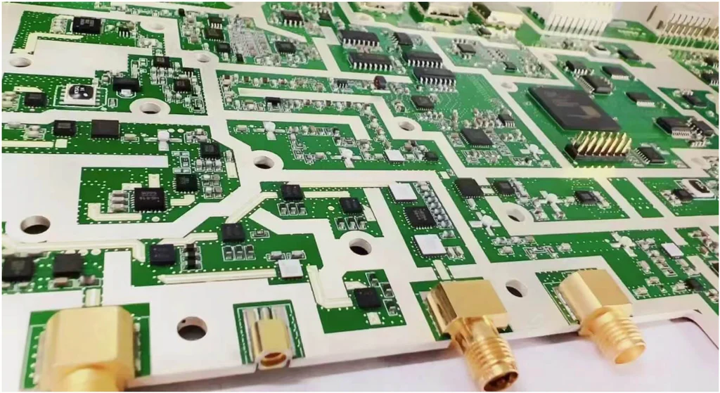
Rogers PCB refers to a family of high-performance laminates optimized for RF and microwave circuits. These materials typically consist of ceramic-filled hydrocarbons or reinforced composites, differing significantly from standard FR-4 substrates. Unlike FR-4, which exhibits higher dielectric losses at gigahertz frequencies, Rogers PCBs maintain low dielectric loss, making them essential for wireless communication. In RF design, low dielectric loss preserves signal power and reduces attenuation over transmission lines. For antenna design, stable electrical properties enable consistent radiation patterns and impedance matching.
The relevance of Rogers PCB in wireless communication stems from the escalating frequency bands in modern systems. Devices operating in Wi-Fi 6, 5G sub-6 GHz, or mmWave require substrates that minimize insertion loss and support high data rates. Poor material choice leads to increased heat generation and degraded efficiency, compromising device reliability. Rogers PCBs provide the dimensional stability and low dissipation factor needed for compact, high-density layouts. Engineers must prioritize these materials when signal paths exceed a few gigahertz to avoid performance bottlenecks.
Technical Principles Behind Rogers PCB Performance
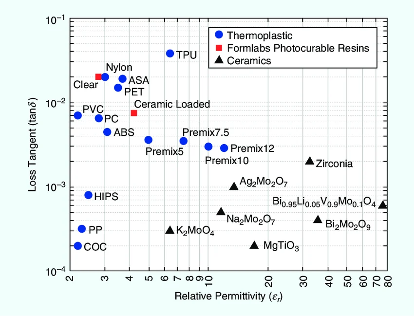
The core of Rogers PCB superiority lies in its dielectric properties, primarily the dielectric constant (Dk) and dissipation factor (Df). Dk influences signal propagation speed and trace width calculations in RF design; lower, stable Dk values around 3.0 allow for controlled impedance without excessive linewidths. Df, often termed loss tangent, quantifies energy dissipation as heat; ultra-low Df in Rogers materials, typically below 0.004 at 10 GHz, ensures minimal attenuation in long traces or antennas. These properties remain consistent across frequency and temperature ranges, critical for wireless devices exposed to varying environments.
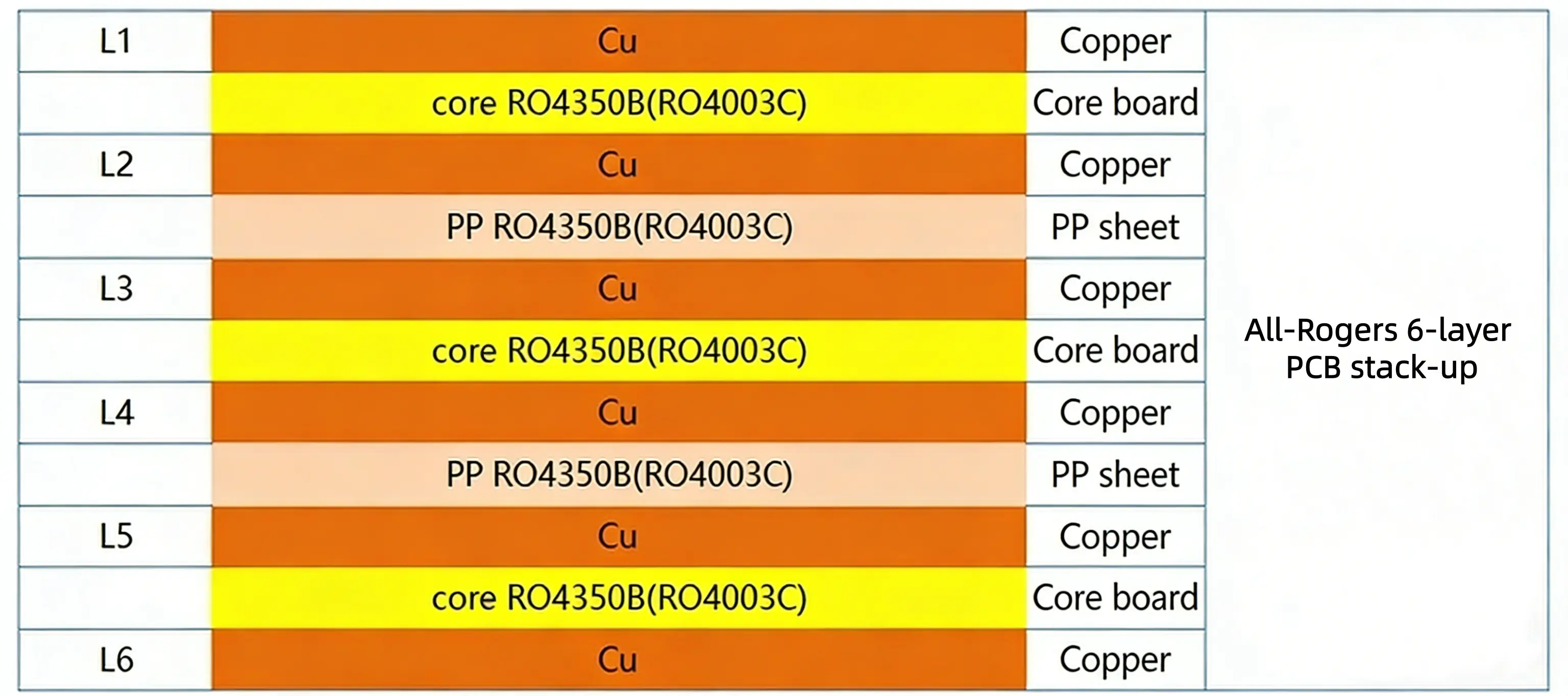
Thermal management further distinguishes Rogers PCBs. Low coefficients of thermal expansion (CTE) in the Z-axis prevent warpage during soldering or operation, aligning with IPC-6012E qualification standards for rigid printed boards. This stability supports multilayer stacks where RF and digital signals coexist. Mechanical robustness allows compatibility with standard fabrication processes, reducing yield issues. In antenna design, low passive intermodulation (PIM) arises from smooth surfaces and pure dielectrics, vital for base station performance.
Surface roughness and conductor properties interact with the substrate to optimize skin effect losses at high frequencies. Rogers laminates pair well with low-profile copper foils, further lowering insertion loss. Moisture absorption remains negligible, preserving Dk stability per IPC-A-600K acceptability criteria. These mechanisms collectively enable Rogers PCB to excel in demanding wireless applications.
Key Factors in Choosing the Right Rogers PCB for Your Design
Selecting a Rogers PCB begins with defining operational frequency and power levels. For sub-6 GHz wireless communication like Wi-Fi routers, materials with moderate Dk suffice, balancing cost and performance. Higher mmWave bands demand ultra-low Df grades to combat severe attenuation. Engineers should model insertion loss using field solvers, targeting less than 0.5 dB per inch at design frequency. Hybrid stacks combining Rogers cores with FR-4 for DC sections optimize cost without RF compromise.
Fabrication compatibility guides material choice. Many Rogers grades process like FR-4, supporting standard lamination and drilling, though some require adjusted parameters for vias. Low Z-axis CTE minimizes via barrel cracking under thermal cycling, adhering to JEDEC J-STD-020E moisture sensitivity guidelines. Cost escalates with lower Df or tighter Dk tolerances, so prototype with simulation data. For antenna design, prioritize low PIM materials to ensure clean spectrum output.
Layout best practices enhance Rogers PCB effectiveness. Maintain 50-ohm microstrip or stripline for RF paths, accounting for Dk variation. Ground planes shield against crosstalk, while cavity structures integrate antennas seamlessly. Thermal vias dissipate power amplifier heat efficiently. Post-fabrication, verify performance via vector network analyzer sweeps against IPC standards. These steps ensure the selected Rogers PCB delivers on low dielectric loss promises.
Applications and Best Practices in RF and Antenna Design
In wireless communication devices, Rogers PCB shines in phased array antennas for 5G base stations. Low loss supports beamforming with minimal phase errors across elements. For consumer routers, compact patch antennas benefit from stable Dk, achieving wide bandwidths. Power amplifiers pair with high thermal conductivity grades to handle kilowatt outputs without degradation.
Troubleshooting common issues involves material-property alignment. Excessive insertion loss signals mismatched Dk; recalibrate models with measured values. Warpage in multilayers points to CTE mismatch, resolvable via symmetric stacks. Antenna detuning from humidity underscores low absorption importance. Best practices include early material qualification per industry standards and iterative prototyping.
Designers often employ simulation-to-fabrication workflows. Extract effective Dk from TRL calibration for accuracy. Via transitions demand optimized stub lengths to preserve return loss. These structured approaches maximize Rogers PCB potential in RF design.
Conclusion
Rogers PCB materials provide indispensable advantages for wireless communication through low dielectric loss, stable Dk, and robust thermal properties. Engineers must evaluate frequency, power, and fabrication needs to select the optimal grade, ensuring superior RF and antenna performance. Adhering to standards like IPC-6012E and IPC-A-600K guarantees reliability. Hybrid designs and precise modeling further unlock benefits. Ultimately, the right Rogers PCB choice elevates device efficiency and market readiness.
FAQs
Q1: What makes Rogers PCB ideal for RF design in wireless communication?
A1: Rogers PCB excels in RF design due to its low dielectric loss and stable dielectric constant, minimizing signal attenuation at high frequencies. This supports precise impedance control and efficient power transfer in wireless devices. Compared to FR-4, it reduces insertion loss by orders of magnitude, per standard testing methods. Engineers achieve better yield in antenna design with these properties.
Q2: How does low dielectric loss impact antenna design on Rogers PCB?
A2: Low dielectric loss in Rogers PCB preserves radiated power, enhancing antenna efficiency and gain in wireless communication. It cuts heat dissipation, allowing denser arrays without thermal throttling. Stable performance across bands ensures reliable MIMO operation. Select grades with Df below 0.004 for mmWave antennas.
Q3: When should electric engineers choose Rogers PCB over standard materials for wireless devices?
A3: Opt for Rogers PCB in wireless devices operating above 2 GHz, where standard materials suffer high loss. It suits 5G, radar, and high-speed Wi-Fi needing low dielectric loss. Cost-benefit analysis favors it for performance-critical paths. Fabrication aligns with IPC guidelines for seamless integration.
Q4: What standards apply to Rogers PCB fabrication for RF applications?
A4: IPC-6012E qualifies rigid boards for performance, including Rogers laminates in RF contexts. IPC-A-600K sets visual and dimensional acceptability criteria. JEDEC J-STD-020E handles moisture sensitivity during reflow. These ensure quality in wireless communication PCBs.
References
IPC-6012E — Qualification and Performance Specification for Rigid Printed Boards. IPC, 2017
IPC-A-600K — Acceptability of Printed Boards. IPC, 2020
JEDEC J-STD-020E — Moisture/Reflow Sensitivity Classification. JEDEC, 2014


