 ALLPCB


Introduction
Electronic hobbyists often seek hands-on projects that blend circuit design with advanced materials to explore high-frequency performance. Building a simple RF amplifier circuit using Rogers PCB stands out as an excellent DIY RF project, allowing you to amplify weak radio signals while learning critical high-frequency amplifier design techniques. Rogers PCB materials excel in RF applications due to their low dielectric loss and dimensional stability, making them ideal for frequencies above 500 MHz where standard FR-4 falls short. This project guides you through schematic creation, RF PCB layout, and assembly, emphasizing practical steps for reliable results. By the end, you will have a functional amplifier suitable for experimentation in receivers or transmitters.
What Is an RF Amplifier and Why Use Rogers PCB?
An RF amplifier circuit boosts low-level radio frequency signals to higher power levels while preserving signal integrity across a specific bandwidth. In hobbyist contexts, these amplifiers find use in radio receivers, signal generators, and test equipment, where even small losses can degrade performance. Rogers PCB projects leverage specialized laminates with consistent dielectric constants and low loss tangents, ensuring minimal signal attenuation at microwave frequencies. Unlike general-purpose substrates, Rogers materials maintain performance under varying temperatures and humidity, crucial for repeatable DIY RF projects. Choosing Rogers PCB for high-frequency amplifier design prevents issues like phase shifts or excessive insertion loss that plague standard boards. This combination empowers hobbyists to achieve professional-grade results in compact forms.
Key Principles of High-Frequency Amplifier Design
High-frequency amplifier design revolves around impedance matching, gain stability, and minimizing parasitic effects inherent to RF signals. At RF frequencies, transmission line effects dominate, requiring traces to act as controlled impedance lines rather than simple wires. A basic RF amplifier circuit often employs a single transistor in common-emitter or common-source configuration, with input and output matching networks to maximize power transfer. Feedback resistors or networks enhance broadband response, while bias circuits ensure linear operation without distortion. Designers must calculate trace widths using the substrate's dielectric constant to achieve 50-ohm impedance, a standard for most RF systems. Adhering to principles like these forms the foundation for successful Rogers PCB projects.
Stability remains paramount, as unintended oscillations can destroy components or mask true gain. Unconditional stability factors, such as K greater than 1 and delta less than 1 across the band, guide transistor selection and network tuning. Thermal management also plays a role, with heat spreaders or vias dissipating power from the active device. In DIY RF projects, simulations help predict behavior before fabrication, though empirical tuning refines the final product. These mechanisms ensure the amplifier delivers clean gain without spurs or harmonics.
Designing the RF Amplifier Circuit
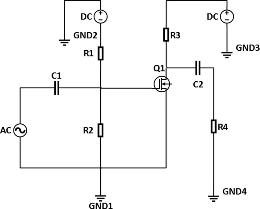
Start with a straightforward single-stage RF amplifier circuit using a bipolar junction transistor (BJT) or field-effect transistor (FET) capable of handling your target frequency, say 1-2 GHz. The schematic includes an input pi-network for matching the source to the transistor gate or base, followed by the amplifying device biased at a quiescent point for Class A operation. Output features another pi-network transforming the low transistor impedance to 50 ohms, with DC blocking capacitors isolating RF from bias. A simple resistive feedback from collector to base provides gain flattening and stability over 20-30 dB bandwidth. Power supply decoupling capacitors near the transistor prevent oscillations from supply noise. This topology suits electronic hobbyists new to RF PCB layout.
Component values derive from Smith chart analysis or basic formulas, ensuring conjugate matching at center frequency. For instance, inductors and capacitors form low-pass pi sections, calculated via standard RF formulas without needing complex software. Bias resistors set collector current around 10-20 mA for low noise, while emitter degeneration improves linearity. Simulate the small-signal S-parameters to verify 10-15 dB gain and return loss better than 10 dB. Once verified, export the netlist for PCB layout. This methodical approach minimizes iterations in high-frequency amplifier design.
RF PCB Layout Best Practices
RF PCB layout demands meticulous planning to preserve signal integrity on Rogers substrates. Begin with a solid ground plane on the bottom layer, stitched with vias every lambda/20 to form an effective RF return path. Traces function as microstrip lines, with widths computed for 50-ohm impedance using the formula Z0 = (87 / sqrt(Er + 1.41)) * ln(5.98h / (0.8w + t)), where Er is the dielectric constant around 3.0-3.5 for Rogers materials, h is substrate height, w trace width, t copper thickness. Keep RF paths short and straight, avoiding right angles that cause reflections; use 45-degree bends or curves instead. Place the transistor centrally with minimal via usage under RF paths to reduce inductance.
Power and ground separation prevents coupling, with DC lines routed away from RF traces and decoupled locally. Via fencing around sensitive areas confines fields, while coplanar waveguide options suit higher powers. IPC-2221B provides generic guidelines for trace spacing and clearance in high-frequency boards, ensuring manufacturability. For multilayer Rogers PCB projects, symmetric stackups control warpage and maintain impedance. Fabricate with controlled impedance tolerances under 10% for repeatable performance. These practices elevate DIY RF projects to reliable standards.
Component placement follows signal flow: input match, transistor, output match in a straight line to minimize parasitics. SMD parts with RF ratings reduce lead inductance, soldered per J-STD-001G requirements for high-frequency joints. Thermal reliefs under pads aid soldering without stressing the Rogers material. Post-layout extraction verifies parasitics before committing to production. Hobbyists benefit from these steps, achieving low VSWR across the band.
Assembly and Testing Your RF Amplifier
Assembly begins with preparing the Rogers PCB, which requires careful handling due to its thin copper and rigid nature. Stencil printing or manual solder paste application suits low-volume hobbyist work, followed by reflow or hot air soldering for SMD parts. Hand-solder the transistor last to avoid heat damage, using flux and low-temperature profiles compatible with Rogers laminates. Install SMA connectors for input/output, ensuring ground continuity. Power up gradually with current limiting to verify bias points match design.
Testing involves a vector network analyzer (VNA) for S-parameters, measuring gain, return loss, and isolation. Expect flat gain response and input/output match better than -10 dB. A spectrum analyzer checks for spurious outputs under driven conditions. Tune matching networks with trimmer caps if needed for optimization. Common metrics include P1dB compression and noise figure, targeted under 3 dB for low-noise amps. Document results to iterate future Rogers PCB projects.
Troubleshooting Common Issues in DIY RF Projects
Oscillations often stem from poor grounding or inadequate decoupling; add more vias and 100 pF caps across supply pins. Low gain points to impedance mismatch, verified by probing return loss and adjusting network values. Excessive loss suggests trace losses or substrate issues, mitigated by wider traces or lower-loss Rogers grades. Overheating requires better thermal vias or heat sinks on the transistor flange. IPC-6012E qualification specs guide inspection for defects like delamination post-assembly. Systematic debugging with a VNA resolves most high-frequency amplifier design pitfalls.
Conclusion
Building a simple RF amplifier circuit on Rogers PCB offers electronic hobbyists a rewarding entry into high-frequency amplifier design. Key takeaways include precise impedance-controlled RF PCB layout, stable biasing, and adherence to layout best practices for minimal losses. Rogers materials shine in DIY RF projects by enabling GHz performance without exotic tools. Experiment with variations like multi-stage configs for higher gain. This project builds skills transferable to antennas, filters, and beyond. Start small, measure often, and enjoy the RF realm.
FAQs
Q1: What makes Rogers PCB ideal for an RF amplifier circuit?
A1: Rogers PCB projects benefit from low loss tangent and stable dielectric constant, reducing signal attenuation at high frequencies. In high-frequency amplifier design, this ensures flat gain and low phase noise across bands like 1-6 GHz. Hobbyists appreciate the material's machinability for prototypes. Proper handling prevents warpage during assembly.
Q2: How do I optimize RF PCB layout for a DIY RF project?
A2: Focus on 50-ohm microstrip traces, solid ground planes with via stitching, and linear signal paths in RF PCB layout. Place components along the flow to cut parasitics, and separate DC from RF. IPC-2221B offers spacing rules for reliability. Test iteratively for best results.
Q3: What are common mistakes in high-frequency amplifier design?
A3: Mismatches cause reflections and low gain; always simulate matching networks. Poor grounding leads to oscillations, fixed by via fences. Overlooking thermal paths overheats devices. In Rogers PCB projects, verify stackup symmetry for stability.
Q4: Can beginners tackle a simple RF amplifier circuit?
A4: Yes, start with a single-transistor design and basic tools like a VNA. Follow structured steps for schematic, layout, and test. Rogers PCB simplifies high-freq due to low loss. Gain practical RF skills through measurement and tweak.
References
IPC-2221B — Generic Standard on Printed Board Design. IPC, 2012
IPC-6012E — Qualification and Performance Specification for Rigid Printed Boards. IPC, 2017
J-STD-001G — Requirements for Soldered Electrical and Electronic Assemblies. IPC, 2011
IPC-2252 — Design Guide for RF/Microwave Circuit Boards. IPC, 2003


