 ALLPCB


When it comes to designing a printed circuit board (PCB), one of the key decisions you'll face is whether to use a symmetrical or asymmetrical stackup. If you're wondering whether an asymmetrical stackup is right for your PCB, the answer depends on your project's specific needs. Asymmetrical stackups can offer flexibility in design and potential cost savings, but they come with challenges like uneven thermal expansion and manufacturing complexities. On the other hand, symmetrical stackups provide balance and stability, often making them a safer choice for most applications. In this comprehensive analysis, we'll dive deep into the asymmetrical stackup comparison, explore symmetrical vs asymmetrical stackup differences, and provide insights into PCB design best practices and PCB cost analysis to help you make an informed decision.
What Is a PCB Stackup and Why Does It Matter?
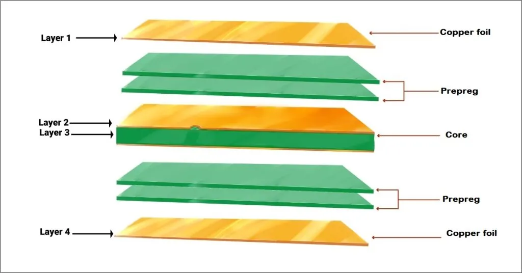
A PCB stackup refers to the arrangement of conductive copper layers and insulating materials (like prepreg and core) that make up a multilayer PCB. These layers include signal layers for routing traces, power planes for distributing voltage, and ground planes for shielding and noise reduction. The way these layers are organized—whether symmetrically or asymmetrically—plays a critical role in the board's performance, manufacturability, and cost.
The stackup design directly impacts signal integrity, electromagnetic compatibility (EMC), PCB thermal management, and mechanical stability. A well-planned stackup can minimize issues like crosstalk, impedance mismatches, and warping, while a poorly designed one can lead to costly redesigns or product failures. Understanding the differences between symmetrical and asymmetrical stackups is the first step in optimizing your PCB for performance and budget.
Symmetrical vs Asymmetrical Stackup: Key Differences
Before diving into the pros and cons, let's define these two stackup types and highlight their core differences.
What Is a Symmetrical Stackup?
A symmetrical stackup is designed with an even balance of layers above and below the center of the board. For example, in an 8-layer PCB, you might have four layers on top and four on the bottom, with copper and dielectric materials distributed evenly. This balance mirrors the structure on both sides, ensuring uniform thickness and material properties.
What Is an Asymmetrical Stackup?
An asymmetrical stackup, on the other hand, lacks this balance. The layers are not evenly distributed, meaning one side of the board may have more copper or dielectric material than the other. For instance, a 6-layer PCB might have four layers on one side and two on the other, creating an uneven structure.
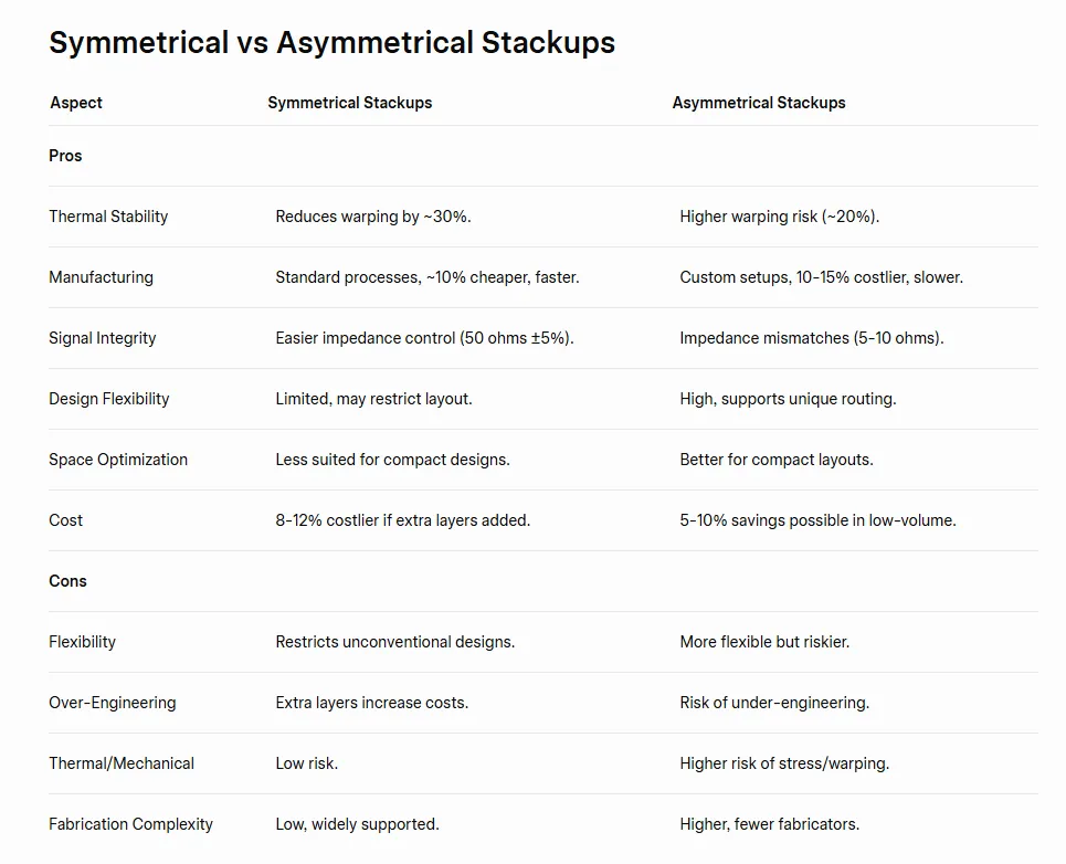
Core Differences at a Glance
- Layer Distribution: Symmetrical stackups have balanced layers; asymmetrical ones do not.
- Thermal Expansion: Symmetrical designs expand evenly under heat, while asymmetrical designs may warp due to uneven stress.
- Manufacturing Complexity: Symmetrical stackups are often easier and cheaper to produce, while asymmetrical ones may require specialized processes.
- Application Suitability: Symmetrical stackups suit most standard designs; asymmetrical ones are used for specific needs like unique routing or space constraints.
Advantages and Disadvantages of Asymmetrical Stackups
Now that we understand the basics, let's explore the benefits and drawbacks of opting for an asymmetrical stackup in your PCB design.
Advantages of Asymmetrical Stackups
- Design Flexibility: Asymmetrical stackups allow designers to prioritize specific layers (like high-speed signal layers) on one side of the board, accommodating unique routing requirements or component placement.
- Space Optimization: In compact designs, an asymmetrical stackup can help fit more functionality into limited space by unevenly distributing layers to match the layout needs.
- Potential Cost Savings: In some cases, reducing the number of layers on one side can lower material costs, though this depends on manufacturing capabilities and volume. For instance, a design with fewer total layers on one side might save on copper and dielectric material, potentially reducing costs by 5-10% in low-volume production runs.
Disadvantages of Asymmetrical Stackups
- Thermal and Mechanical Issues: Uneven layer distribution can lead to differential thermal expansion, causing the board to warp during soldering or operation. Warping risks can increase by up to 20% in asymmetrical designs under high-temperature conditions (e.g., reflow soldering at 260°C).
- Manufacturing Challenges: Many fabrication houses prefer symmetrical designs due to standardized processes. Asymmetrical stackups may require custom setups, increasing lead times and costs by 10-15% for small batches.
- Signal Integrity Risks: Uneven distribution can complicate impedance control, especially for high-speed signals (above 1 GHz), potentially leading to mismatches of 5-10 ohms if not carefully managed.
Advantages and Disadvantages of Symmetrical Stackups
For a balanced perspective in this asymmetrical stackup comparison, let’s look at the strengths and weaknesses of symmetrical stackups.
Advantages of Symmetrical Stackups
- Thermal Stability: Balanced layers ensure uniform expansion and contraction, reducing the risk of warping by as much as 30% compared to asymmetrical designs under thermal stress.
- Easier Manufacturing: Symmetrical designs align with standard fabrication processes, often resulting in lower costs (up to 10% savings) and faster turnaround times.
- Better Signal Integrity: Symmetrical stackups simplify impedance matching and reduce crosstalk, making them ideal for high-speed designs with tight tolerances (e.g., controlled impedance of 50 ohms ±5%).
Disadvantages of Symmetrical Stackups
- Limited Flexibility: Symmetrical designs may force compromises in routing or component placement, especially for unconventional layouts.
- Potential Over-Engineering: Adding layers just to maintain symmetry can increase costs unnecessarily, sometimes by 8-12% in material expenses for small runs.
PCB Design Best Practices: Choosing the Right Stackup
Selecting between symmetrical and asymmetrical stackups requires careful consideration of your project's goals. Here are some PCB design best practices to guide your decision.
1. Assess Your Application Needs
Start by evaluating the electrical, mechanical, and thermal requirements of your PCB. For high-speed designs (e.g., data rates above 5 Gbps), symmetrical stackups are often better due to consistent impedance control. For space-constrained or custom designs, an asymmetrical stackup might offer the flexibility you need.
2. Prioritize Signal Integrity
Signal integrity is critical, especially for modern electronics with high-frequency signals. Use simulation tools to model impedance and crosstalk. For instance, maintaining a differential pair impedance of 100 ohms in USB 3.0 designs is easier with a symmetrical stackup due to uniform layer spacing.
3. Consider Thermal Management
If your PCB will operate in harsh environments or undergo multiple soldering cycles, symmetrical stackups reduce the risk of warping. Studies show that asymmetrical designs can experience up to 0.5 mm of bowing in a 100 mm x 100 mm board under thermal stress, compared to 0.2 mm for symmetrical ones.
4. Collaborate with Your Manufacturer
Early communication with your fabrication partner is essential. Some manufacturers may charge premiums for asymmetrical stackups due to additional processing steps. Discuss stackup options to align your design with their capabilities and avoid unexpected costs or delays.
PCB Cost Analysis: Symmetrical vs Asymmetrical Stackups
Cost is a significant factor in any PCB project. Let’s break down the PCB cost analysis for both stackup types to help you budget effectively.
Material Costs
Symmetrical stackups often use more consistent materials across layers, which can streamline procurement and reduce expenses. Asymmetrical designs might save on material by reducing layer count on one side, but custom dielectric thickness can offset these savings. On average, material costs for asymmetrical stackups can be 5-8% higher due to non-standard configurations.
Manufacturing Costs
Fabrication costs for symmetrical stackups are typically lower because they align with standard processes. For a 6-layer board, a symmetrical design might cost $50 per square foot in small volumes, while an asymmetrical design could rise to $55-$60 due to additional setup time. In high-volume production, these differences narrow but still impact overall expenses.
Yield and Reliability Impact
Asymmetrical stackups may have lower yields due to manufacturing defects like warping or delamination, potentially increasing costs by 3-5% due to rework or scrap. Symmetrical stackups, with higher reliability, minimize these risks, saving money in the long run.
When Should You Choose an Asymmetrical Stackup?
While symmetrical stackups are the default choice for most projects, there are scenarios where an asymmetrical stackup makes sense:
- Unique Routing Needs: If your design requires specific layers to be closer to one surface (e.g., for RF components operating at 2.4 GHz), an asymmetrical stackup can accommodate this.
- Compact Designs: In ultra-small devices like wearables, asymmetrical stackups can help fit complex circuitry into limited space.
- Cost-Driven Prototyping: For early prototypes where cost outweighs long-term reliability, an asymmetrical design might reduce initial expenses.
However, always weigh these benefits against potential risks like thermal instability and manufacturing challenges. If in doubt, a symmetrical stackup is often the safer, more reliable option.
Final Thoughts on Asymmetrical vs Symmetrical Stackups
Choosing between an asymmetrical and symmetrical stackup is a critical decision that impacts your PCB's performance, reliability, and cost. While asymmetrical stackups offer flexibility for specialized designs, they come with trade-offs in thermal stability and manufacturing complexity. Symmetrical stackups, by contrast, provide balance and ease of production, making them suitable for most applications.
By following PCB design best practices—such as assessing application needs, prioritizing signal integrity, and collaborating with your manufacturer—you can make an informed choice. Additionally, a thorough PCB cost analysis ensures that your decision aligns with your budget. Whether you opt for an asymmetrical or symmetrical stackup, the key is to tailor your design to the specific demands of your project.
At ALLPCB, we’re committed to supporting your PCB design journey with expert guidance and high-quality manufacturing solutions. Dive into the details of symmetrical vs asymmetrical stackup options, and let us help you bring your vision to life with precision and efficiency.


