 ALLPCB


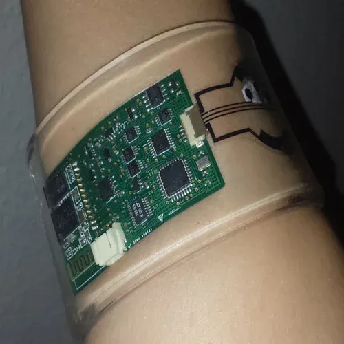
In the fast-evolving world of wearable health technology, printed circuit boards (PCBs) need to be compact, efficient, and reliable. One of the best ways to achieve this is by employing blind via PCB design and buried via PCB design. These advanced via technologies allow designers to increase circuit density and improve routing efficiency, which are critical for small, high-performance devices like fitness trackers, smartwatches, and medical monitoring systems. In this blog, we’ll explore how blind and buried vias, along with techniques like microvia drilling and via-in-pad technology, can transform PCB design for wearable health applications. We’ll dive deep into their benefits, applications, and best practices for implementation.
What Are Blind and Buried Vias in PCB Design?
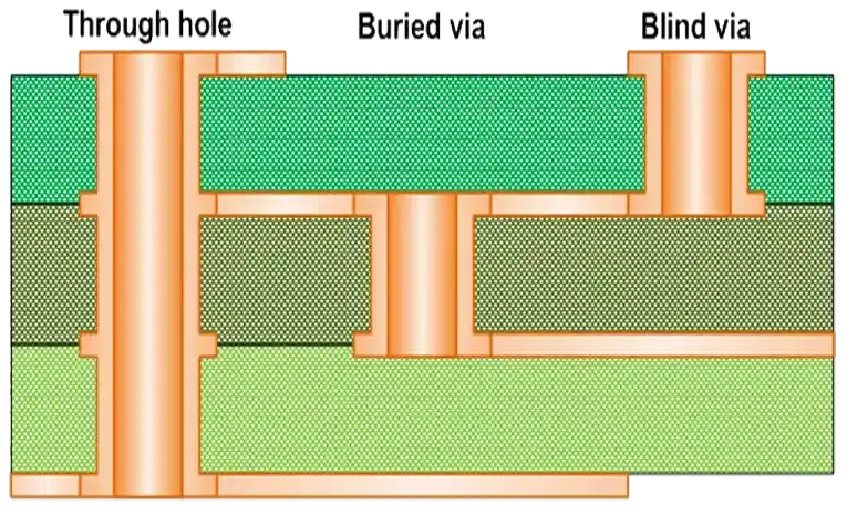
Before we get into the specifics of wearable health PCBs, let’s clarify what blind and buried vias are. Vias are small holes in a PCB that connect different layers of the board, allowing electrical signals to pass through. Traditional through-hole vias go all the way from the top to the bottom of the board, but blind and buried vias are different.
- Blind Vias: These connect the outermost layer of a PCB to one or more inner layers but do not go through the entire board. For example, a blind via might link the top layer to the second layer without reaching the bottom.
- Buried Vias: These are located entirely within the inner layers of the PCB and do not connect to the outer surfaces. They might connect layer 2 to layer 3 in a multilayer board, staying hidden inside.
Both types of vias are key in HDI PCB via design (High-Density Interconnect), which focuses on packing more components into smaller spaces. By using blind and buried vias, designers can save space on the outer layers, reduce signal interference, and create more efficient routing paths.
Why Use Blind and Buried Vias in Wearable Health PCBs?
Wearable health devices, such as heart rate monitors or glucose sensors, have unique design challenges. They must be small enough to wear comfortably, yet powerful enough to process data in real-time. Here’s why blind and buried vias are a game-changer for these applications:
1. Increased Circuit Density
Wearable devices often have limited space, sometimes as small as a few square centimeters. Blind and buried vias allow for more connections in a smaller area since they don’t take up space on all layers. This means you can fit more components, like sensors and microcontrollers, onto the board without increasing its size.
2. Improved Routing Efficiency
Routing traces in a compact PCB can be tricky, especially when dealing with high-speed signals. Blind and buried vias free up space on the outer layers for critical components and reduce the need for long, winding traces. This results in shorter signal paths, which can improve performance by reducing signal delay and loss. For instance, a shorter trace might reduce signal propagation delay by 10-20% in high-speed designs.
3. Reduced Signal Interference
In wearable health devices, signal integrity is vital. These devices often handle sensitive data, like heart rate readings, where even small interference can lead to inaccurate results. By keeping vias hidden or limited to specific layers, blind and buried vias minimize crosstalk and electromagnetic interference (EMI). This is especially important when working with analog signals, which are prone to noise.
4. Support for Miniaturization
The trend in wearable tech is clear: smaller is better. Blind and buried vias, often paired with microvia drilling techniques, enable designers to create multilayer boards with fine-pitch components. Microvias, which are tiny vias with diameters as small as 0.1 mm, further enhance density by allowing precise connections in tight spaces.
How Blind and Buried Vias Fit into HDI PCB Design
HDI PCB via design is at the heart of modern wearable technology. HDI stands for High-Density Interconnect, and it refers to PCBs with a higher wiring density per unit area than traditional boards. This is achieved through the use of smaller vias, finer traces, and advanced manufacturing techniques.
Blind and buried vias are essential in HDI designs because they allow for more layers to be interconnected without increasing the board’s footprint. For example, a typical HDI board for a wearable device might have 6-8 layers, with blind vias connecting the top layer to inner signal layers and buried vias handling internal connections. This layered approach not only saves space but also improves thermal management by distributing heat across multiple layers.
Additionally, HDI designs often use stacked or staggered vias. Stacked vias are multiple blind or buried vias aligned on the same center, while staggered vias are offset. Stacked vias can reduce parasitic capacitance by up to 15%, improving signal integrity for high-frequency applications like wireless data transmission in health wearables.
Microvia Drilling Techniques for Precision and Reliability
One of the key technologies behind blind and buried vias is microvia drilling techniques. Microvias are small-diameter vias, often drilled using lasers, that enable high-density connections in HDI PCBs. Here’s why microvia drilling is critical for wearable health PCBs:
- Precision: Laser drilling can create vias with diameters as small as 0.075 mm, allowing for ultra-fine connections in compact designs.
- Reliability: Microvias have a lower aspect ratio (depth-to-diameter ratio) compared to traditional vias, often around 0.8:1, which reduces the risk of plating defects and improves durability.
- Flexibility: Microvias can be used as blind or buried vias, making them versatile for multilayer boards in wearable devices.
However, microvia drilling requires advanced manufacturing capabilities. The process must ensure clean, debris-free holes to avoid signal issues. For wearable health PCBs, where reliability can be a matter of life and death, choosing a manufacturer with expertise in microvia technology is crucial.
Via-in-Pad Technology: A Perfect Match for Wearable Health PCBs
Another innovative approach that complements blind and buried vias is via-in-pad technology. This technique places vias directly under component pads, typically for surface-mount devices (SMDs) like ball grid arrays (BGAs) or chip-scale packages (CSPs). Here’s how it benefits wearable health PCB design:
- Space Savings: By placing vias under pads, you eliminate the need for additional space around components, allowing for tighter layouts. This is ideal for tiny wearables where every millimeter counts.
- Better Signal Performance: Via-in-pad reduces trace length between components and vias, lowering inductance and improving high-speed signal transmission. For instance, this can reduce signal loss by up to 5% in high-frequency circuits.
- Enhanced Thermal Management: Vias under pads can act as thermal conduits, dissipating heat from components like processors or power management chips, which are common in health wearables.
However, via-in-pad requires careful design to avoid manufacturing issues like solder wicking, where solder flows into the via during assembly. Using plugged or filled vias can prevent this, ensuring a reliable connection. When combined with blind vias, via-in-pad technology can further optimize space and performance in HDI designs.
Challenges and Best Practices for Implementing Blind and Buried Vias
While blind and buried vias offer many advantages, they come with challenges that designers must address to ensure success in wearable health PCBs.
Challenges:
- Higher Manufacturing Costs: Creating blind and buried vias, especially with microvia drilling, is more complex and costly than standard through-hole vias. This can impact the overall budget for a project.
- Design Complexity: Routing with multiple via types requires advanced software and expertise to avoid errors like misalignment or signal interference.
- Reliability Concerns: If not manufactured correctly, blind and buried vias can suffer from issues like incomplete plating, leading to connection failures. This is critical for health devices where reliability is non-negotiable.
Best Practices:
- Optimize Layer Stackup: Plan your PCB layer stackup early in the design process to determine where blind and buried vias are most effective. For example, place high-speed signals on inner layers connected by buried vias to minimize interference.
- Use Design for Manufacturability (DFM) Guidelines: Work closely with your PCB manufacturer to follow their DFM rules, ensuring that via sizes, aspect ratios, and spacing meet production capabilities.
- Test Signal Integrity: Use simulation tools to analyze signal integrity and impedance before finalizing the design. For wearable health devices, aim for controlled impedance values (e.g., 50 ohms for RF signals) to ensure accurate data transmission.
- Choose Reliable Materials: Select high-quality PCB materials with low dielectric constants (e.g., 3.5-4.0) to support high-frequency signals and reduce signal loss in HDI designs.
Real-World Applications in Wearable Health Technology
The use of blind and buried vias in wearable health PCBs is already making a significant impact. Consider a smartwatch that monitors heart rate and blood oxygen levels. The PCB inside must handle multiple sensors, a processor, wireless communication, and a battery management system—all within a tiny form factor. Blind vias connect the outer layer components to inner signal layers, while buried vias manage internal routing for power and ground planes, reducing noise and saving space.
Similarly, in wearable insulin monitors, HDI designs with microvias ensure precise connections for analog sensors, maintaining signal accuracy for life-critical readings. Via-in-pad technology allows the placement of compact BGAs for processing units, ensuring the device remains small enough to wear discreetly.
Conclusion: The Future of Wearable Health PCBs with Advanced Via Technologies
As wearable health technology continues to advance, the demand for smaller, more efficient PCBs will only grow. Employing blind via PCB design and buried via PCB design offers a powerful solution to meet these demands, enhancing density and routing efficiency in ways traditional vias cannot. When combined with microvia drilling techniques, HDI PCB via design, and via-in-pad technology, these approaches enable designers to create cutting-edge devices that are both compact and reliable.
At ALLPCB, we’re committed to supporting engineers in pushing the boundaries of wearable health technology. By leveraging advanced via technologies and following best practices, you can design PCBs that meet the unique challenges of this field. Whether you’re working on a fitness tracker or a medical monitoring system, the right via strategy can make all the difference in achieving high performance in a small package.


