 ALLPCB


If you're new to PCB design and wondering how to get started with Eagle PCB design software, you're in the right place. This beginner's guide to Eagle will walk you through the essentials of using this powerful tool, from creating a schematic in Eagle to designing a PCB layout in Eagle. Whether you're a hobbyist or an aspiring engineer, this Eagle PCB design tutorial will help you build your first circuit board with confidence. Let’s dive into the step-by-step process and explore how to make the most of this software for your projects.
Why Choose Eagle for PCB Design?
Eagle PCB design software is a popular choice among beginners and professionals alike for designing printed circuit boards. Known for its user-friendly interface and robust features, it offers a free version that’s perfect for small projects or learning the basics. With Eagle, you can create detailed schematics and turn them into functional PCB layouts, making it an ideal starting point for anyone entering the world of electronics design.
In this guide, we’ll break down the key features of Eagle and provide a clear path for beginners to follow. By the end, you’ll understand how to navigate the software, design a simple circuit, and prepare your files for manufacturing.
Getting Started with Eagle PCB Design Software
Before you start designing, you need to install Eagle and set up your workspace. Here’s how to begin your journey with this beginner's guide to Eagle:
- Download and Install Eagle: Visit the official website to download the free version of Eagle. Follow the installation instructions for your operating system (Windows, macOS, or Linux). The free version supports boards up to 100 cm2, which is enough for most beginner projects.
- Familiarize Yourself with the Interface: When you open Eagle, you’ll see two main editors: the Schematic Editor and the Board Editor. The Schematic Editor is where you design the circuit diagram, while the Board Editor is for creating the physical PCB layout in Eagle.
- Set Up Libraries: Eagle comes with a library of components like resistors, capacitors, and microcontrollers. You can also add custom libraries if you need specific parts for your design.
Step 1: Creating a Schematic in Eagle
The first step in any PCB design project is creating a schematic in Eagle. A schematic is like a blueprint of your circuit, showing how components are connected electrically. Follow these steps to build your first schematic:
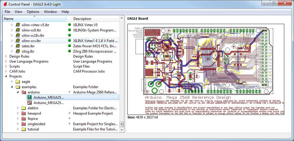
- Create a New Project: In Eagle, go to the Control Panel, right-click on “Projects,” and select “New Project.” Name your project something relevant, like “LED_Circuit.”
- Open the Schematic Editor: Right-click your project and select “New Schematic.” This opens a blank canvas where you’ll draw your circuit.
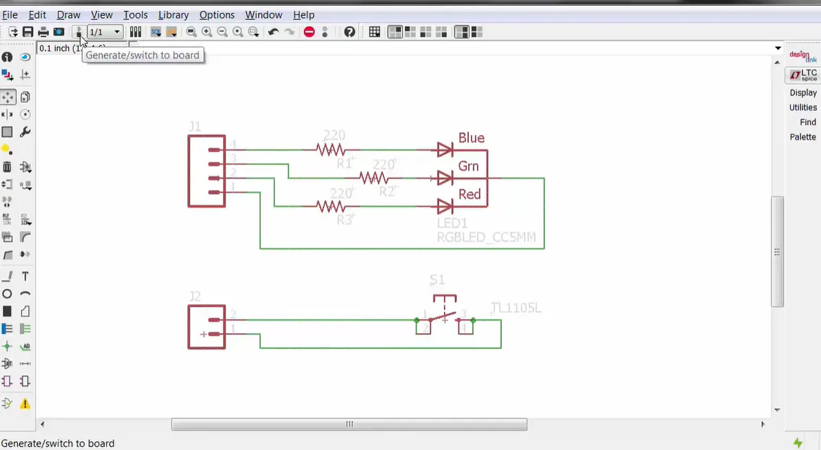
- Add Components: Use the “Add Part” tool (or type “add” in the command line) to search for components from the library. For a simple circuit, you might add a 5V power supply, a 220-ohm resistor, and an LED.
- Connect Components: Use the “Net” tool to draw wires connecting the components. For example, connect the positive terminal of the power supply to one end of the resistor, then connect the other end of the resistor to the anode of the LED, and finally connect the cathode of the LED to ground.
- Label Nets: Labeling nets (wires) makes your schematic easier to read. Use the “Label” tool to name connections like “VCC” for power or “GND” for ground.
- Check for Errors: Run the Electrical Rule Check (ERC) by clicking the “ERC” button. This tool identifies issues like unconnected pins or missing power supplies. Fix any errors before moving to the next step.
A well-designed schematic is crucial because it directly impacts the PCB layout. For instance, if you’re designing a circuit with high-speed signals (like a 100 MHz clock), ensure that your schematic reflects proper grounding to avoid signal integrity issues later.
Step 2: Designing a PCB Layout in Eagle
Once your schematic is ready, the next step in this Eagle PCB design tutorial is to create the PCB layout in Eagle. This is where you arrange the physical components on the board and route the copper traces that connect them.
- Switch to Board Editor: Click the “Generate/Switch to Board” button in the Schematic Editor. Eagle will create a new board file linked to your schematic. You’ll see all your components placed outside the board outline initially.
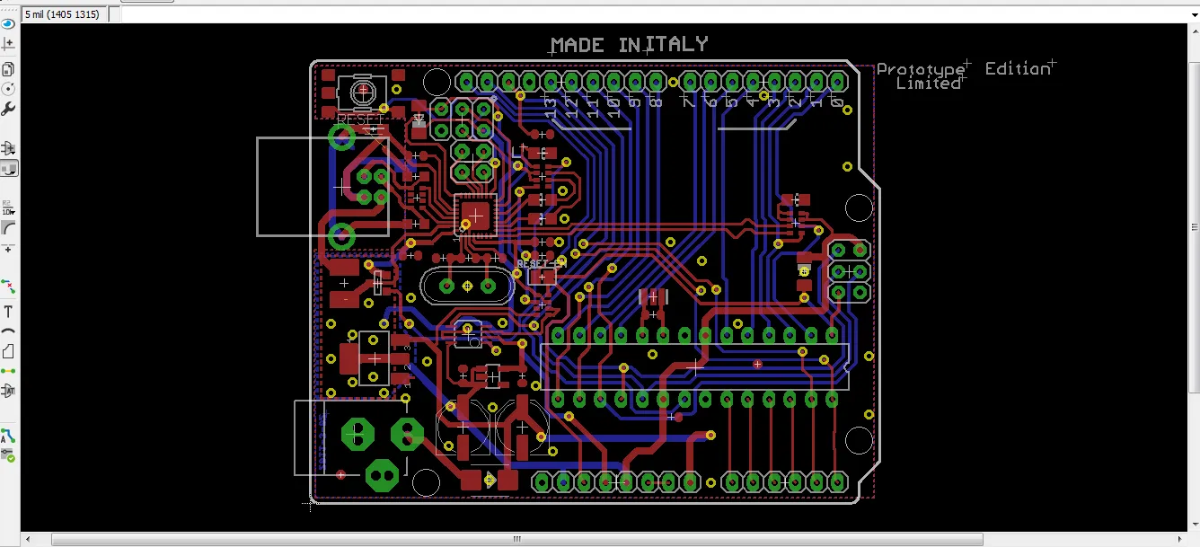
- Define Board Dimensions: Use the “Move” tool to drag the board outline to the desired size. For a small project, a 5 cm x 5 cm board might be enough. Use the “Dimension” layer to set the exact size.
- Place Components: Drag each component inside the board outline. Place them logically—for example, keep power components near the input and sensitive components away from noisy areas. Eagle shows “airwires” (yellow lines) indicating connections that need to be routed.
- Route Traces: Use the “Route” tool to draw copper traces between components, following the airwires. For a simple design, stick to a single-layer board. Ensure traces are at least 0.254 mm (10 mils) wide for standard current levels (up to 1A). For high-current paths, increase the width to 0.5 mm or more to handle the load (e.g., a 2A path at 5V).
- Add Ground Plane: Create a ground plane using the “Polygon” tool on the bottom layer. Name it “GND” to connect it to all ground pins automatically. This reduces noise, especially in circuits with frequencies above 1 MHz.
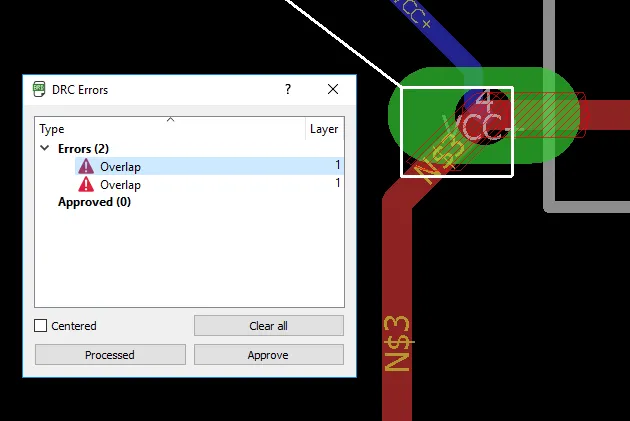
- Run Design Rule Check (DRC): Click the “DRC” button to check for errors like overlapping traces or insufficient clearances. Set clearance values to at least 0.2 mm for standard designs to avoid manufacturing issues.
Designing a PCB layout in Eagle requires attention to detail. For example, if you’re working on a circuit with impedance-controlled traces (like a 50-ohm line for RF signals), use Eagle’s trace width calculator to match the impedance based on your board’s dielectric constant (typically 4.5 for FR4 material).
Step 3: Preparing Your Design for Manufacturing
After completing your PCB layout in Eagle, the final step is to prepare your design files for manufacturing. Eagle makes this process straightforward with tools to generate the necessary files.
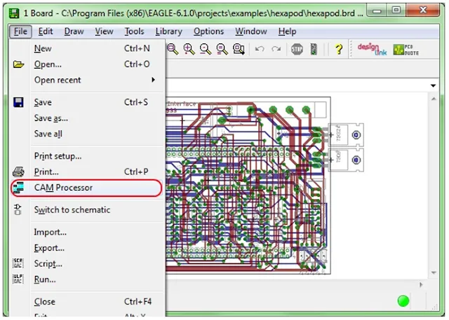
- Generate Gerber Files: Go to the Board Editor and click “CAM Processor.” Load a CAM job file (often provided by manufacturers) to generate Gerber files. These files include layers like top copper, bottom copper, solder mask, and silkscreen. Typically, you’ll generate 6-8 files depending on your board’s complexity.
- Create a Bill of Materials (BOM): Use Eagle’s “BOM” tool to export a list of components used in your design. This file helps manufacturers know which parts to source for assembly.
- Export Drill Files: In the CAM Processor, ensure drill files (in Excellon format) are generated. These files specify the locations and sizes of holes for vias and mounting.
- Review Your Files: Use a Gerber viewer tool to check your files for errors before sending them to a manufacturer. Look for misaligned layers or missing traces.
Ensuring your files are correct is critical. A small error, like a 0.1 mm misalignment in drill holes, can render your board unusable. Double-check all settings, especially if your design includes fine-pitch components with pin spacings below 0.5 mm.
Tips for Success with Eagle PCB Design Software
As you continue learning through this beginner's guide to Eagle, keep these tips in mind to improve your skills and avoid common pitfalls:
- Start Simple: Begin with basic circuits, like a single LED with a resistor, before tackling complex designs with microcontrollers or high-speed signals.
- Use Shortcuts: Eagle supports keyboard shortcuts (like “M” for Move and “R” for Route) to speed up your workflow. Check the help menu for a full list.
- Leverage Community Resources: The Eagle user community offers tutorials, forums, and custom libraries. If you’re stuck, search for solutions shared by other users.
- Optimize for Signal Integrity: For designs with fast-switching signals (e.g., 10 MHz or higher), keep trace lengths short (under 10 cm) to minimize delays and crosstalk.
- Save Often: Eagle doesn’t autosave by default, so save your work frequently to avoid losing progress during crashes.
Common Challenges and How to Overcome Them
Beginners often face hurdles when using Eagle PCB design software. Here are some common issues and solutions:
- Component Not Found in Library: If a part isn’t in Eagle’s default library, search online for user-created libraries or create your own using the Library Editor.
- Routing Errors: If airwires won’t route, check for locked components or insufficient board space. Use the “Ripup” tool to undo traces and try again.
- DRC Errors: Clearance or width violations often occur in dense designs. Adjust trace widths (e.g., reduce to 0.2 mm for low-current signals) or increase board size to resolve these.
Conclusion: Mastering Eagle for Your PCB Projects
Learning how to use Eagle PCB design software opens up a world of possibilities for creating custom electronics. This Eagle PCB design tutorial has guided you through the essentials—creating a schematic in Eagle, designing a PCB layout in Eagle, and preparing files for manufacturing. With practice, you’ll gain confidence in handling more complex designs and optimizing your circuits for performance.
Start with small projects to build your skills, and don’t hesitate to explore additional resources within the Eagle community. As a beginner, every step you take brings you closer to mastering PCB design. Keep experimenting, and soon you’ll be designing boards that power innovative solutions.


