 ALLPCB


Designing high-voltage printed circuit boards requires careful attention to detail to prevent dangerous issues like electrical arcing. One of the most critical factors in ensuring safety and performance is optimizing component spacing on high-voltage PCBs. Proper spacing helps avoid arcing, ensures reliable operation, and meets industry standards. In this comprehensive guide, we'll explore the essentials of component spacing for high-voltage PCBs, dive into layout guidelines, and share practical tips for preventing arcing. Whether you're an engineer working on power electronics or a designer tackling high-voltage applications, this post will provide actionable insights to enhance your designs.
Why Component Spacing Matters in High-Voltage PCB Design
When dealing with high-voltage PCBs, the risk of electrical arcing—a sudden discharge of electricity through the air between conductive elements—becomes a major concern. Arcing can damage components, cause short circuits, or even lead to fires. The primary way to prevent this is by maintaining adequate spacing between components and traces carrying high voltages. Proper component spacing on high-voltage PCBs ensures that the electric field strength between conductors doesn't exceed the breakdown voltage of the surrounding material, typically air or the PCB substrate.
Beyond safety, spacing also impacts the overall performance and reliability of the board. Insufficient spacing can lead to electromagnetic interference (EMI), crosstalk, or unintended capacitance between traces. By following high-voltage PCB layout guidelines, you can minimize these risks and create designs that are both safe and efficient.
Key Terms to Understand
Before diving deeper, let's clarify two essential concepts related to spacing in high-voltage PCB design:
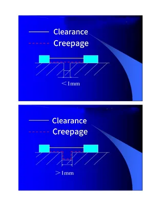
- Clearance: The shortest distance through the air between two conductive elements. This is critical for preventing arcing in high-voltage designs.
- Creepage: The shortest path along the surface of the insulating material between two conductive elements. This is important for preventing surface discharges, especially in humid or contaminated environments.
Both clearance and creepage distances must be calculated based on the voltage levels, environmental conditions, and applicable standards like IPC-2221 or IEC 60950. For example, at 500V, a typical clearance distance might be around 2.5 mm, while creepage could require 3.2 mm or more, depending on the material and pollution degree.
Recommended Reading: Creepage and Clearance: The MVPs of High-Voltage PCB Spacing
Core Principles of Component Spacing for High-Voltage PCBs
Optimizing component spacing on high-voltage PCBs involves balancing safety, functionality, and manufacturability. Below are the core principles to follow when designing your layout to prevent arcing and ensure reliability.
1. Adhere to Voltage-Based Spacing Standards
The spacing between components and traces must be determined by the voltage levels in your circuit. Higher voltages require larger distances to prevent breakdown. Industry standards provide specific guidelines for minimum spacing. For instance, according to IPC-2221B, the clearance for voltages between 301-500V should be at least 0.25 mm per 100V, meaning a 400V difference would require a 1.0 mm clearance under ideal conditions. However, for safety-critical applications, these values are often doubled or adjusted based on altitude and environmental factors.
Always check the specific standards relevant to your project. Over-spacing can unnecessarily increase board size, while under-spacing risks arcing and failure. Use design software with built-in design rule checks (DRC) to enforce these spacing rules during layout.
2. Consider Environmental Factors
The environment where the PCB will operate plays a big role in determining spacing. High humidity, dust, or pollution can reduce the insulating properties of air and surfaces, increasing the risk of arcing or surface discharge. In such cases, creepage distances must be larger. For example, in a pollution degree 2 environment (typical industrial settings), creepage distances for 500V might need to be 4.0 mm or more, compared to 2.5 mm in a clean, controlled environment.
Altitude also affects clearance distances because air pressure decreases at higher elevations, lowering its dielectric strength. For designs operating above 2000 meters, clearance distances may need to be increased by 10-20% to account for this.
3. Group Components by Voltage Levels
One effective strategy for component placement on high-voltage PCBs is to group components based on their operating voltage. Keep high-voltage components and traces away from low-voltage sections to minimize the risk of arcing across large potential differences. For instance, place high-voltage power transistors or capacitors in one area of the board, while isolating control circuitry or low-voltage signals in another. Use physical barriers like slots or insulating materials if needed to further separate these zones.
4. Minimize Sharp Edges and Points
Sharp edges or pointed traces can concentrate electric fields, increasing the likelihood of arcing. When designing high-voltage PCB layouts, use rounded corners for traces and pads wherever possible. This reduces the electric field intensity and helps maintain a uniform distribution of voltage stress. For example, instead of a 90-degree corner on a high-voltage trace, use a 45-degree chamfer or a smooth curve.
High-Voltage PCB Layout Guidelines for Preventing Arcing
Now that we've covered the basic principles of component spacing, let's dive into specific high-voltage PCB layout guidelines that will help you design safer and more reliable boards. These tips focus on practical steps you can take during the design phase to prevent arcing and optimize performance.
1. Use Wider Traces for High-Voltage Lines
High-voltage traces often carry significant current, which can generate heat and increase the risk of breakdown if traces are too narrow. Wider traces not only handle current better but also allow for greater spacing from adjacent conductors. As a rule of thumb, for every 1A of current, a trace should be at least 0.5 mm wide on a standard 1 oz copper layer. For high-voltage applications, consider increasing this width further to reduce resistance and heat buildup.
2. Avoid Placing Components Under High-Voltage Traces
Placing components directly under high-voltage traces or pads can create unintended paths for arcing, especially if the board experiences mechanical stress or contamination. Always route high-voltage traces away from sensitive components, and use inner layers or shielding if crossing is unavoidable. If components must be near high-voltage areas, ensure that clearance and creepage distances are strictly maintained.
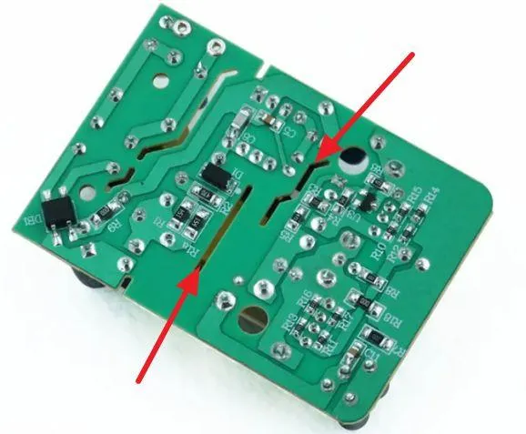
3. Incorporate Slots and Barriers for Extra Protection
In extremely high-voltage designs (above 1000V), consider adding physical barriers like slots or cutouts in the PCB to increase creepage distances. Slots can be particularly effective between high-voltage pads or traces, as they force any surface discharge to travel a longer path. For example, a 1.6 mm slot between two pads rated for 1500V can significantly reduce the risk of arcing. Insulating materials or conformal coatings can also be applied to further enhance protection.
4. Test for Dielectric Strength
After completing your layout, simulate or test the dielectric strength of your PCB material and spacing. The dielectric strength of standard FR-4 material is approximately 20 kV/mm, but this can vary based on manufacturing quality and environmental conditions. Ensure that your design doesn't push the material beyond its limits. For critical applications, consider using high-voltage-specific laminates with higher dielectric strength, such as polyimide-based materials.
Suggested Reading: Optimizing PCB Layout for High-Voltage Connectors in EV Battery Management Systems
Best Practices for Component Placement on High-Voltage PCBs
Effective component placement on high-voltage PCBs goes hand-in-hand with spacing to prevent arcing and ensure a robust design. Here are some best practices to follow during the placement phase.
1. Prioritize Accessibility for Heat Dissipation
High-voltage components like power transistors or diodes often generate significant heat. Place these components in areas with good airflow or near heatsinks to prevent thermal buildup, which can degrade insulation and increase arcing risk. Avoid clustering heat-generating components together unless adequate cooling is provided.
2. Maintain Uniform Spacing Across the Board
Consistency in spacing helps avoid weak points in your design. Use design software to set uniform clearance and creepage rules for all high-voltage nets. For instance, if your design requires a 3 mm clearance for 600V, apply this rule across all relevant traces and components to eliminate guesswork and reduce errors.
3. Isolate Sensitive Components
Components like microcontrollers or sensors are often sensitive to noise and voltage spikes. Place these away from high-voltage areas to prevent interference and potential damage. If isolation isn't possible due to space constraints, use shielding techniques or optocouplers to separate high and low-voltage domains electrically.
Common Mistakes to Avoid in High-Voltage PCB Design
Even experienced designers can make errors when working with high-voltage PCBs. Here are some common pitfalls to watch out for when optimizing component spacing and layout.
1. Underestimating Creepage Distances
Many designers focus on clearance but overlook creepage, especially in humid or dirty environments. Always calculate creepage distances based on the expected operating conditions and material properties. Failing to do so can lead to surface discharges that compromise the board's safety.
2. Ignoring Manufacturing Tolerances
Designs that meet spacing requirements on paper may fail in production due to manufacturing tolerances. For example, a trace-to-trace clearance of 2.0 mm might be reduced to 1.8 mm due to etching inaccuracies. Account for these tolerances by adding a safety margin (e.g., 10-20%) to your spacing rules.
3. Overcrowding the Board
Attempting to minimize board size by packing components too closely can lead to insufficient spacing and increased arcing risk. While compact designs are desirable, safety must always come first in high-voltage applications. Allocate enough space for proper spacing, even if it means using a larger board.
Tools and Resources for High-Voltage PCB Design
Designing high-voltage PCBs with optimal component spacing is easier with the right tools and resources. Many modern design software platforms offer features like automated spacing checks and simulation tools to help identify potential issues before manufacturing. Look for software that supports design rule constraints (DRC) tailored to high-voltage standards. Additionally, refer to industry resources like IPC standards or IEC guidelines for detailed spacing charts and environmental considerations.
Conclusion: Building Safer High-Voltage PCBs with Proper Spacing
Optimizing component spacing on high-voltage PCBs is a fundamental step in preventing arcing and ensuring the safety and reliability of your designs. By adhering to voltage-based spacing standards, considering environmental factors, and following high-voltage PCB layout guidelines, you can minimize risks and create boards that perform consistently under demanding conditions. Thoughtful component placement on high-voltage PCBs, combined with practical strategies like using slots or wider traces, further enhances your design's robustness.
Whether you're working on power supplies, industrial equipment, or renewable energy systems, mastering component spacing for high-voltage PCBs is a skill that pays off in safer, more efficient designs. Take the time to apply these principles in your next project, and you'll be well on your way to creating high-performing, arc-free PCBs that stand the test of time.


