ALLPCB


In the world of electronics, protecting printed circuit boards (PCBs) from damage is crucial for ensuring long-term reliability and performance. PCB potting or encapsulation is a process that envelopes the PCB electronics in a protective material, often a resin or silicone compound, to shield them from environmental hazards like moisture spray, dust, chemicals, and physical stress. This blog post will dive deep into what PCB potting and encapsulation are, why they matter, the processes involved, and their benefits for safeguarding electronics in challenging conditions.
Whether you're an engineer designing a product for harsh environments or a manufacturer looking to enhance the durability of your devices, understanding this protective technique can make a significant difference. Let’s explore the details of PCB potting and encapsulation, breaking it down into easy-to-understand sections with practical insights and data.
Understanding PCB Potting and Encapsulation: The Basics
PCB potting and encapsulation refer to the process of encasing electronic components or an entire PCB assembly in a solid or gelatinous material. The primary goal is to create a barrier that protects the delicate electronics from external threats. While the terms "potting" and "encapsulation" are often used interchangeably, they can have slight differences depending on the context. Potting typically involves filling a complete assembly within a shell or "pot," while encapsulation might refer to coating individual components.
The materials used for this process, such as epoxy resins, silicone gels, or polyurethane compounds, harden after application to form a protective layer. This layer not only guards against moisture spray and other environmental hazards but also enhances the structural integrity of the PCB by reducing the impact of vibrations and shocks.
Why is PCB Potting or Encapsulation Necessary?
Electronics are often exposed to conditions that can degrade their performance or cause complete failure. From industrial machinery operating in humid environments to automotive systems facing temperature extremes, unprotected PCBs are vulnerable. Here are some key reasons why potting or encapsulation is essential:
- Protection from Moisture and Water: Moisture spray or humidity can cause short circuits or corrosion on a PCB. Potting creates a watertight seal that prevents water ingress, ensuring the electronics remain functional even in damp conditions.
- Defense Against Environmental Hazards: Dust, dirt, and corrosive chemicals are common environmental hazards that can damage exposed components. A protective layer keeps these elements out, extending the lifespan of the device.
- Shock and Vibration Resistance: In applications like aerospace or automotive systems, PCBs face constant vibrations or sudden impacts. Potting absorbs mechanical stress, reducing the risk of loose connections or cracked components.
- Thermal Management: Some potting compounds help dissipate heat, protecting components from overheating. For instance, certain epoxy resins have thermal conductivity values ranging from 0.2 to 1.5 W/m·K, aiding in heat transfer away from critical areas.
- Prevention of Electrical Issues: Potting materials with high dielectric strength (often exceeding 20 kV/mm for epoxies) prevent electrical arcing or corona discharge in high-voltage applications, ensuring safety and reliability.
By addressing these challenges, potting ensures that electronics can operate reliably in harsh environments, from underwater sensors to outdoor communication equipment.
Materials Used in PCB Potting and Encapsulation
The choice of material for potting or encapsulation depends on the specific requirements of the application, such as temperature range, flexibility, or chemical resistance. Here are the most common materials used to envelope the PCB electronics:
- Epoxy Resins: Known for their excellent mechanical strength and adhesion, epoxy resins are widely used. They offer high resistance to moisture and chemicals, with dielectric strengths often around 15-25 kV/mm. However, they can be rigid and may crack under extreme thermal cycling.
- Silicone Gels: Silicone is flexible and ideal for applications requiring thermal expansion or vibration damping. It operates well in a wide temperature range (typically -60°C to 200°C) and provides good protection against moisture spray.
- Polyurethane Compounds: These materials balance flexibility and toughness, making them suitable for outdoor applications exposed to varying weather conditions. They also resist abrasion and impact.
Each material has its pros and cons, and selecting the right one often involves considering factors like curing time, cost, and environmental exposure. For instance, a device exposed to constant moisture spray might benefit from a silicone compound due to its superior water resistance.
The PCB Potting and Encapsulation Process
The process of potting or encapsulation is meticulous to ensure complete coverage without damaging the electronics. Here’s a step-by-step breakdown of how it’s typically done:
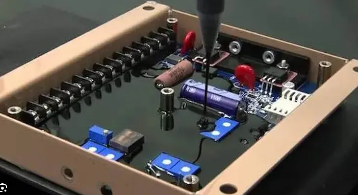
- Preparation: The PCB assembly is cleaned to remove any contaminants like dust or grease that could interfere with adhesion. Components are inspected to ensure they are securely mounted.
- Placement in a Shell or Mold: The PCB is placed into a container, often called a "pot," which will hold the liquid compound. This shell can be part of the final product housing or a temporary mold.
- Mixing the Compound: The potting material, such as a two-part epoxy, is mixed according to the manufacturer’s specifications. This often involves combining a resin and a hardener in precise ratios to initiate curing.
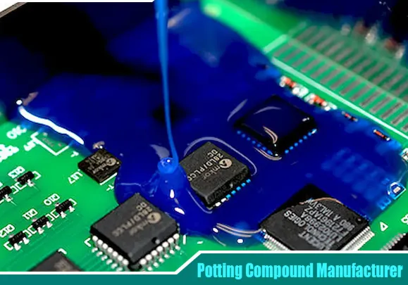
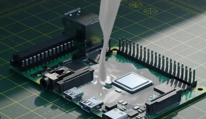
- Pouring and Filling: The liquid compound is slowly poured over the PCB to envelope the PCB electronics completely. This step is done carefully to avoid air bubbles, which could compromise the protective layer. Vacuum degassing may be used to remove trapped air.
- Curing: The assembly is left to cure, often for 24-48 hours, depending on the material. Curing can take place at room temperature or in a controlled environment with specific humidity and temperature settings (e.g., 25°C and 50% relative humidity for some epoxies).
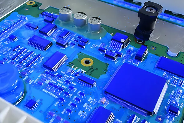
- Inspection: After curing, the potted PCB is inspected for gaps, bubbles, or incomplete coverage. Accessibility to connectors or ports is also verified to ensure functionality isn’t impaired.
This process, when done with precision, creates a robust shield against environmental hazards and ensures the electronics remain operational under stress.
Benefits of PCB Potting and Encapsulation
The advantages of potting or encapsulation go beyond basic protection. Here are some detailed benefits that make this process a go-to solution for many industries:
- Enhanced Durability: A potted PCB can withstand harsh conditions, such as exposure to moisture spray in marine environments or corrosive gases in industrial settings. This durability can extend the lifespan of a device by years.
- Improved Reliability: By preventing failures caused by environmental factors, potting reduces downtime and maintenance costs. For example, a study in industrial electronics showed that potted assemblies had a 30% lower failure rate in humid conditions compared to unprotected ones.
- Compact Design Support: Potting can eliminate the need for bulky enclosures, allowing for smaller, lighter designs while still protecting against environmental hazards.
- Security Against Tampering: Encapsulation can deter reverse engineering by making it difficult to access internal components without damaging the assembly. This is particularly valuable for proprietary or sensitive electronics.
These benefits make potting an ideal choice for applications ranging from consumer electronics to critical systems in aerospace and medical devices.
Applications of PCB Potting and Encapsulation
Potting and encapsulation are used across various industries where electronics face challenging conditions. Here are a few examples:
- Automotive: Control units and sensors in vehicles are potted to resist vibrations, temperature swings (from -40°C to 125°C), and exposure to road spray or fluids.
- Marine: Electronics on ships or underwater equipment are encapsulated to prevent damage from saltwater and constant moisture spray.
- Industrial: Machinery in factories often operates in dusty or chemically aggressive environments. Potting protects control boards from these environmental hazards.
- Medical: Devices like portable monitors or implants need protection from bodily fluids and sterilization processes, making encapsulation critical.
Challenges and Considerations in PCB Potting
While potting offers significant advantages, there are challenges to keep in mind during implementation:
- Thermal Expansion: Differences in thermal expansion between the potting material and PCB components can cause stress or cracking. Choosing a material with a compatible coefficient of thermal expansion (CTE), typically in the range of 20-60 ppm/°C for epoxies, is crucial.
- Repairability: Once potted, accessing or repairing components becomes difficult or impossible. Designs must account for this by ensuring reliability before potting.
- Cost: High-quality potting materials and precise application processes can increase production costs, especially for large-scale manufacturing.
Balancing these challenges with the benefits requires careful planning and testing to ensure the potting process meets the specific needs of the application.
Potting vs. Conformal Coating: What’s the Difference?
While both potting and conformal coating protect PCBs, they serve different purposes. Conformal coating is a thin layer (typically 25-75 micrometers) applied to the surface of a PCB to protect against moisture and dust. Potting, on the other hand, completely envelopes the PCB electronics in a thick, solid material for maximum protection against environmental hazards.
Conformal coating is lighter and allows for easier rework, but it offers less protection against heavy impacts or prolonged exposure to moisture spray. Potting is more robust but adds weight and is permanent. Choosing between the two depends on the level of protection needed and the operating environment.
Tips for Effective PCB Potting and Encapsulation
To achieve the best results when potting or encapsulating a PCB, consider these practical tips:
- Material Testing: Test different potting compounds under simulated conditions (e.g., humidity levels of 85% or temperature cycles from -40°C to 85°C) to ensure compatibility with your application.
- Design for Potting: Leave space around critical components for the compound to flow evenly, and ensure connectors remain accessible if needed.
- Control Curing Conditions: Maintain consistent temperature and humidity during curing to avoid defects like incomplete hardening or bubble formation.
- Use Vacuum Degassing: For high-reliability applications, use vacuum equipment to remove air bubbles during the pouring process, ensuring a seamless protective layer.
Conclusion: Safeguarding Electronics with PCB Potting and Encapsulation
PCB potting or encapsulation is a powerful technique to protect electronics from a wide range of threats, including moisture spray and other environmental hazards. By using materials like epoxy, silicone, or polyurethane to envelope the PCB electronics, manufacturers can ensure durability, reliability, and performance even in the harshest conditions. From automotive to marine applications, this process plays a vital role in modern electronics design.
Understanding the materials, processes, and benefits of potting allows engineers and manufacturers to make informed decisions about protecting their products. While challenges like cost and repairability exist, the long-term advantages often outweigh these concerns. With careful planning and execution, PCB potting can be the key to creating robust, long-lasting electronic devices ready to face any environment.