 ALLPCB


Creating a smart home system by designing and assembling your own home appliance control PCBs (Printed Circuit Boards) is an exciting and rewarding project. With the right open-source tools and DIY methods, you can build custom solutions to control lights, fans, or other devices from your smartphone or automated triggers. This guide from ALLPCB dives deep into the process, covering everything from design to assembly. Whether you're curious about the DIY PCB etching process, toner transfer PCB method, photoresist PCB method, CNC PCB milling, or assembling PCBs with reflow soldering and hand soldering, we’ve got you covered. Let’s explore how to use open-source EDA software for PCB design and bring your smart home vision to life!
Why Build Your Own Smart Home PCBs?
Building your own PCBs for smart home appliance control offers unmatched customization. You can tailor circuits to specific needs, like integrating Wi-Fi modules for remote access or sensors for automation. DIY methods save costs for small projects or prototypes compared to commercial boards, and using open-source tools makes the process accessible to everyone. Plus, the hands-on experience sharpens your electronics skills. In this post, we’ll walk through every step, ensuring you have the knowledge to create reliable, functional boards for your smart home setup.
Getting Started: Understanding Smart Home PCB Requirements
Before diving into design and assembly, let’s outline what a typical smart home appliance control PCB needs. These boards often include a microcontroller (like an ESP8266 or ESP32 for Wi-Fi connectivity), relays or MOSFETs to switch appliances on/off, and power regulation circuits (e.g., converting 110-240V AC to 5V DC). A common setup might require a relay rated for 10A at 250V AC to handle household appliances safely. Signal integrity is also key—ensure traces for digital signals (like I2C or SPI) are short, ideally under 10 cm, to minimize interference.
Step 1: Designing Your PCB with Open-Source EDA Software
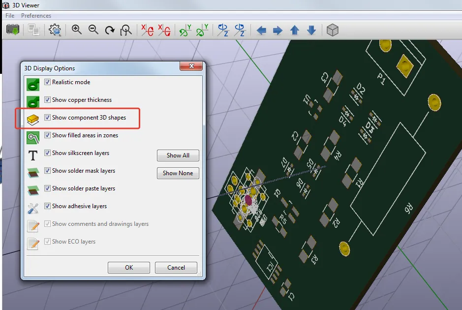
Designing a PCB starts with creating a schematic and layout using Electronic Design Automation (EDA) software. Open-source EDA software for PCB design is a fantastic option for hobbyists and professionals alike, offering powerful features without the cost of premium tools. Popular choices include KiCad, a free suite that supports schematic capture, PCB layout, and 3D visualization. It’s widely used for projects ranging from simple LED circuits to complex IoT devices.
To begin, sketch your circuit in the schematic editor. For a smart home control board, include a microcontroller, a relay module, and necessary resistors and capacitors (e.g., a 10kΩ pull-up resistor for digital pins). Once the schematic is complete, move to the PCB layout editor. Keep high-current traces (like those to the relay) at least 1 mm wide to handle 1-2A safely, and maintain a 0.5 mm clearance between traces to avoid short circuits. KiCad also lets you check design rules to ensure manufacturability.
Step 2: Choosing a DIY PCB Fabrication Method
Once your design is ready, it’s time to fabricate the PCB. DIY methods allow you to create boards at home without waiting for professional manufacturing. Below, we cover four popular techniques: the DIY PCB etching process, toner transfer PCB method, photoresist PCB method, and CNC PCB milling.
Method 1: DIY PCB Etching Process
The DIY PCB etching process is a chemical method to remove unwanted copper from a blank PCB, leaving behind your circuit traces. Start with a copper-clad board and clean it with steel wool to remove oxidation. Print your PCB layout on paper (mirrored), then use an etchant solution like a mix of vinegar, hydrogen peroxide, and salt (a safer alternative to ferric chloride). Submerge the board for 30-60 minutes, agitating occasionally, until excess copper dissolves. Rinse with water and drill holes for components using a 0.8-1.2 mm drill bit.
This method is affordable, with materials costing under $10, but requires caution due to chemical handling. It’s ideal for simple, single-layer boards with trace widths above 0.3 mm.
Method 2: Toner Transfer PCB Method
The toner transfer PCB method uses a laser printer to transfer your design onto the copper board. Print the mirrored PCB layout on glossy paper or transparency film. Place the print face-down on a cleaned copper board and apply heat with an iron at 150-180°C for 5-10 minutes. The toner sticks to the copper, acting as a mask. Soak the board in water to remove paper, then etch with a solution as described above. This method achieves finer traces (down to 0.2 mm) compared to basic etching and works well for detailed smart home control boards.
Method 3: Photoresist PCB Method
The photoresist PCB method offers higher precision for complex designs. Start with a copper board coated with a light-sensitive photoresist layer. Print your layout on a transparency film (not mirrored) and place it over the board. Expose it to UV light for 2-5 minutes—UV nail lamps work well for this. Develop the board in a sodium carbonate solution (1 tsp in 500 ml water) to reveal the pattern, then etch away exposed copper. This method can produce traces as fine as 0.1 mm, making it suitable for densely packed smart home PCBs with multiple components.
Method 4: CNC PCB Milling
For a non-chemical approach, CNC PCB milling uses a computer-controlled router to physically remove copper from the board. Affordable desktop CNC machines, costing $200-500, can mill traces with 0.2 mm precision. Load your PCB design into software like FlatCAM (open-source) to generate toolpaths. Use a 0.1-0.2 mm V-bit for isolation routing and a 1 mm bit for drilling. Milling avoids chemicals, making it safer, but requires an upfront investment in equipment. It’s perfect for quick prototyping of double-sided smart home boards.
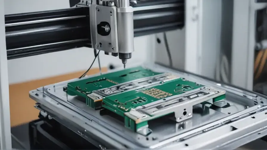
Step 3: Assembling PCBs for Smart Home Control
After fabricating your PCB, the next step is assembly—placing and soldering components onto the board. We’ll explore two methods: assembling PCBs with reflow soldering for surface-mount components and assembling PCBs with hand soldering for through-hole parts.
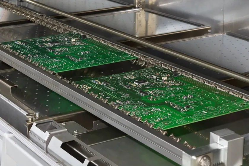
Assembling PCBs with Reflow Soldering
Reflow soldering is ideal for surface-mount devices (SMDs) like microcontrollers or small resistors often used in smart home PCBs. First, apply solder paste to the pads using a stencil or syringe—ensure paste thickness is around 0.1-0.2 mm for even melting. Place components with tweezers, aligning pins precisely with pads. Heat the board in a reflow oven or with a hot air gun at 220-250°C for 1-2 minutes, following a profile of preheat (150°C for 60 seconds), soak, and reflow. The solder paste melts, securing components. Check for cold joints or bridges with a magnifying glass post-cooling.
This method is fast for multiple components but requires equipment like a reflow oven ($50-200 for DIY setups). It’s great for compact smart home designs with SMD Wi-Fi modules.
Assembling PCBs with Hand Soldering
For through-hole components like relays or connectors, hand soldering is the go-to method. Use a soldering iron with a fine tip (1 mm) at 300-350°C. Tin the tip with solder, place the component leads through holes, and apply solder to the pad while touching the iron to both lead and pad for 2-3 seconds. Use 0.5-0.8 mm diameter 60/40 lead solder for easier flow. Trim excess leads with cutters and inspect for shiny, conical joints. Hand soldering is inexpensive (irons start at $10) and perfect for beginners assembling larger smart home control boards.
Step 4: Testing and Programming Your Smart Home PCB
Once assembled, test your PCB for continuity using a multimeter—check that power traces show 0Ω resistance and unrelated pads show infinite resistance to rule out shorts. Power up the board with a 5V supply (or as per design) and measure voltages at key points, like 3.3V at the microcontroller pin. Program the microcontroller with firmware using open-source platforms like the Arduino IDE for ESP8266/ESP32. Upload code to toggle relays via Wi-Fi commands and verify operation by connecting a small load (like a 5W bulb) to the relay output.
Tips for Success in DIY Smart Home PCB Projects
Here are some practical tips to ensure your project goes smoothly:
- Safety First: Wear gloves and goggles during etching or soldering to protect against chemicals and heat.
- Start Simple: Begin with a basic design (e.g., a single relay control) before scaling to multi-device boards.
- Double-Check Designs: Use the design rule check (DRC) in your EDA software to catch errors before fabrication.
- Document Everything: Label components and take photos of each assembly step for troubleshooting.
- Test Incrementally: Assemble and test in stages (e.g., power section first) to isolate issues early.
Conclusion: Building the Future of Your Smart Home
Assembling your own home appliance control PCBs for a DIY smart home is a fulfilling journey that combines creativity and technical skill. By leveraging open-source EDA software for PCB design and mastering techniques like the DIY PCB etching process, toner transfer PCB method, photoresist PCB method, and CNC PCB milling, you can create custom boards tailored to your needs. Whether you’re assembling PCBs with reflow soldering for tiny SMD parts or assembling PCBs with hand soldering for robust relays, these skills empower you to automate and control your living space. With ALLPCB as your guide, dive into this hands-on process and transform your home into a connected, smart environment. Start small, experiment often, and watch your ideas come to life on a copper-clad canvas!


