 ALLPCB


If you're designing a printed circuit board (PCB) with high-density component placement, optimizing the silkscreen layer is crucial for clarity, assembly accuracy, and manufacturability. For small components and dense boards, following specific PCB silkscreen design rules, choosing the right silkscreen font size, and minimizing overlap on SMT pads can make a significant difference. In this comprehensive guide, we'll dive into practical strategies and best practices to achieve an effective silkscreen layout that supports your high-density designs.
What Is PCB Silkscreen and Why Does It Matter for High-Density Designs?
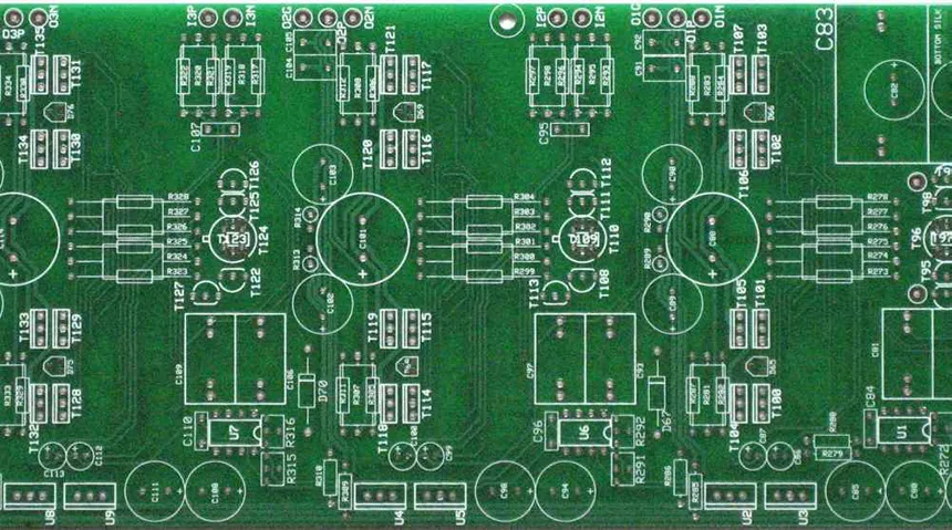
The silkscreen layer on a PCB is the printed text, symbols, and markings that provide essential information for assembly, testing, and debugging. It typically includes component designators, polarity indicators, and other labels that guide technicians during manufacturing and troubleshooting. In high-density designs, where components are packed tightly together, the silkscreen becomes even more critical—and challenging. A poorly designed silkscreen can lead to assembly errors, misinterpretations, or even manufacturing delays.
In dense boards, space is limited, and components like 0402 resistors or tiny ICs leave little room for markings. An optimized silkscreen ensures that information remains legible and functional without interfering with solder pads or other critical areas. Let’s explore how to achieve this balance with actionable design rules and tips.
Key Challenges in Silkscreen Design for High-Density PCBs
Before diving into solutions, it’s important to understand the unique challenges of silkscreen design in high-density layouts:
- Limited Space: With components placed close together, there’s often no room for large or detailed markings.
- Legibility Issues: Small font sizes or crowded text can become unreadable, leading to assembly mistakes.
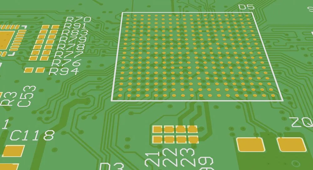
- Overlap with SMT Pads: Silkscreen ink on solder pads can interfere with soldering, causing defects.
- Manufacturing Constraints: Some silkscreen resolutions or line widths may not be supported by all fabrication processes.
Addressing these challenges requires careful planning and adherence to specific design guidelines tailored for small components and dense boards.
PCB Silkscreen Design Rules for Small Components
Designing a silkscreen for small components in high-density layouts demands precision. Here are some essential rules to follow:
1. Prioritize Essential Information
In a crowded layout, you can’t include every detail on the silkscreen. Focus on critical information such as:
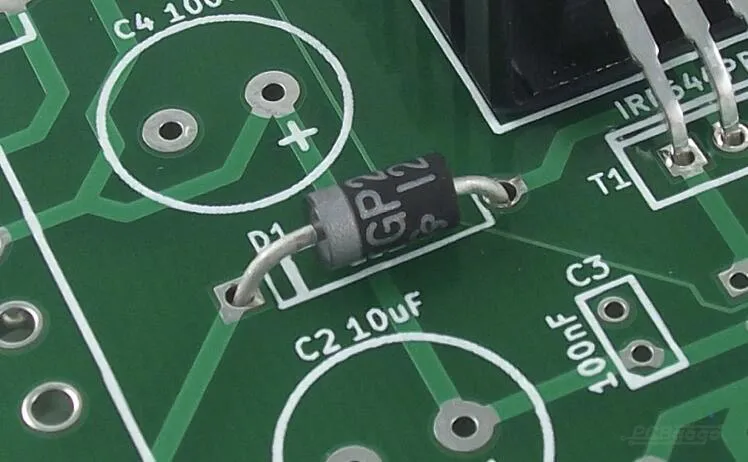
- Component designators (e.g., R1, C2) for identification during assembly.
- Polarity indicators for diodes, capacitors, and ICs to prevent incorrect placement.
- Pin 1 markers for ICs to ensure correct orientation.
Avoid cluttering the board with non-essential text like manufacturer logos or lengthy notes. If additional information is needed, include it in assembly documentation instead of the silkscreen.
2. Use Minimalist Designators
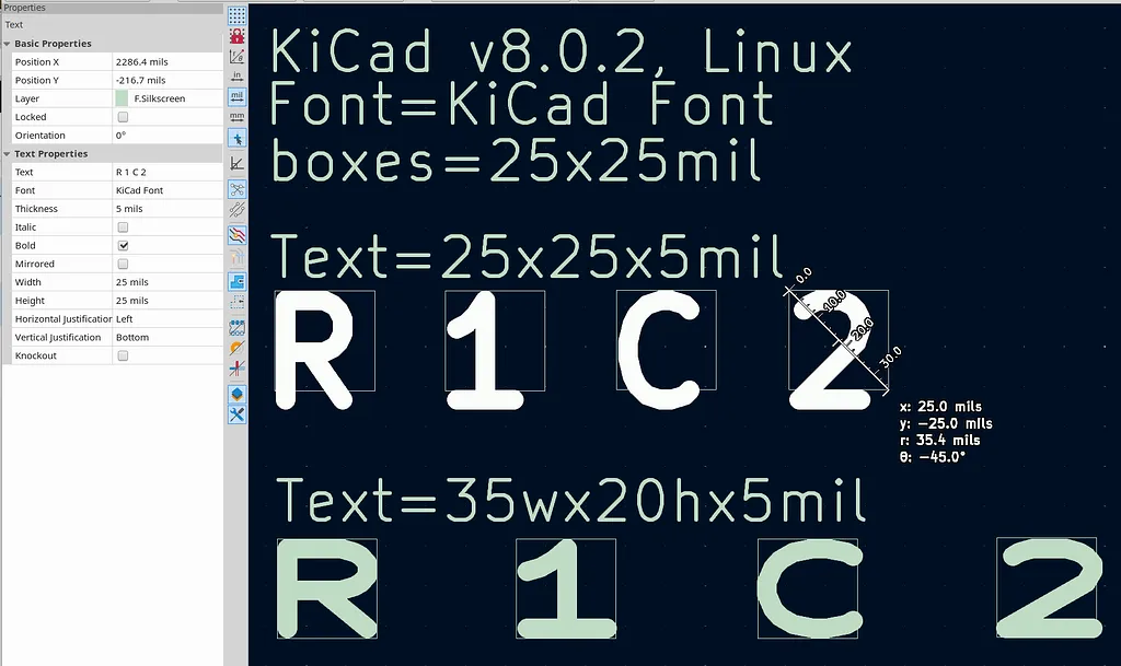
For small components like 0402 or 0201 packages, use short designators. For example, instead of labeling a resistor as “RESISTOR_1K_0402,” simply use “R1.” This saves space and maintains clarity. Ensure that your design software links these designators to a detailed bill of materials (BOM) for reference during assembly.
3. Maintain Uniform Orientation
Place silkscreen text in a consistent direction (e.g., left-to-right or top-to-bottom) to make it easier to read. Avoid rotating text at odd angles unless absolutely necessary, as this can confuse assembly technicians. If space constraints force rotation, limit it to 90-degree
Silkscreen Font Size for Dense Boards
Choosing the right font size is a balancing act between legibility and space constraints. Here’s how to optimize font size for dense boards:
1. Minimum Readable Font Size
The smallest recommended font height for silkscreen text is typically 50 mils (0.050 inches or 1.27 mm) to ensure readability with the naked eye. However, for very dense boards, you might need to go as low as 40 mils (1.016 mm) if space is extremely limited. Be aware that anything smaller may require magnification tools during assembly, which can slow down the process.
Additionally, the line width of the text should be at least 5 mils (0.127 mm) to ensure the ink doesn’t blur or break during printing. Check with your fabrication house for their specific capabilities, as some may have stricter minimums.
2. Adjust Font Style for Clarity
Use simple, sans-serif fonts like Arial or Helvetica for silkscreen text. These fonts are clean and easy to read, even at small sizes. Avoid decorative or complex fonts that can distort during printing or become illegible on dense boards.
3. Test Legibility in Prototypes
Before finalizing your design, order a prototype and inspect the silkscreen under typical assembly conditions. If technicians struggle to read the markings, adjust the font size or spacing in the next revision. This step can save time and reduce errors in full-scale production.
Minimizing Silkscreen Overlap on SMT Pads
One of the most critical aspects of silkscreen design for high-density PCBs is avoiding overlap with surface-mount technology (SMT) pads. Silkscreen ink on pads can interfere with soldering, leading to poor connections or defects. Here’s how to prevent this issue:
1. Maintain Clearance from Solder Pads
Ensure a minimum clearance of 6 mils (0.152 mm) between silkscreen markings and SMT pads. This buffer zone prevents ink from encroaching on areas where solder paste is applied. Some design software includes automated checks for silkscreen-to-pad clearance—use these tools to catch potential issues early.
2. Avoid Placing Text Inside Component Footprints
For small SMT components, resist the temptation to place designators within the component footprint. Instead, position the text adjacent to the component, even if it means using a smaller font or abbreviating the label. If space is too tight, consider moving non-critical markings to a separate assembly drawing.
3. Use Silkscreen Clipping in Design Software
Most PCB design tools allow you to set rules for silkscreen clipping, automatically removing or adjusting text that overlaps with pads or other restricted areas. Configure these settings before finalizing your layout to ensure a clean silkscreen layer.
Additional Tips for Optimizing Silkscreen in High-Density Designs
Beyond the core rules for font size, component placement, and pad clearance, here are some extra strategies to refine your silkscreen design:
1. Choose the Right Silkscreen Color
White is the most common silkscreen color due to its high contrast against green or black solder masks. However, for boards with non-standard mask colors, test different silkscreen shades to ensure visibility. Avoid low-contrast combinations that make text hard to read.
2. Group Markings for Clarity
In areas with multiple small components, group related designators together in a logical pattern. For example, label a row of capacitors as “C1-C5” instead of marking each one individually. This reduces clutter and improves readability.
3. Consider Two-Sided Silkscreen for Double-Sided Boards
If your high-density design uses components on both sides of the board, apply silkscreen to both the top and bottom layers. Clearly distinguish between the two sides in your markings (e.g., prefix bottom-side components with “B_”) to avoid confusion during assembly.
4. Align Silkscreen with Assembly Processes
Work closely with your assembly team to understand their needs. Some automated pick-and-place machines rely on silkscreen markings for component placement, so ensure that critical labels are positioned where they can be easily scanned or read.
Common Silkscreen Mistakes to Avoid in High-Density Designs
Even experienced designers can make errors when working with dense layouts. Watch out for these common pitfalls:
- Overcrowding the Silkscreen: Too much text in a small area leads to unreadable markings. Stick to essential information only.
- Ignoring Manufacturer Guidelines: Failing to follow fabrication limits for line width or text height can result in blurred or missing silkscreen.
- Placing Text Under Components: Markings hidden under larger components are useless. Always position text in visible areas.
- Neglecting Design Rule Checks (DRC): Always run a DRC in your design software to catch silkscreen overlaps or clearance issues before sending files to production.
How Silkscreen Optimization Impacts Manufacturability
A well-designed silkscreen does more than improve readability—it enhances the overall manufacturability of your PCB. Clear markings reduce the risk of assembly errors, speed up manual inspection processes, and minimize costly rework. For high-density designs, where even a single misplaced component can cause a cascade of issues, an optimized silkscreen is a vital part of quality control.
For example, consider a board with 100+ small components packed into a 2-inch by 2-inch area. Without clear silkscreen labels, an assembler might misplace a 0402 capacitor, leading to a short circuit or signal integrity issues. By investing time in silkscreen optimization, you prevent such problems and ensure a smoother production process.
Conclusion: Mastering Silkscreen Design for High-Density PCBs
Optimizing PCB silkscreen for high-density component placement is a critical skill for modern electronics design. By following PCB silkscreen design rules for small components, selecting the appropriate silkscreen font size for dense boards, and minimizing silkscreen overlap on SMT pads, you can create layouts that are both functional and manufacturable. Remember to prioritize essential information, maintain clearance from solder pads, and test legibility in prototypes to achieve the best results.
Whether you’re working on a compact IoT device or a complex multi-layer board, a well-designed silkscreen layer can save time, reduce errors, and improve the overall quality of your PCB. Use the strategies outlined in this guide to refine your approach and take your high-density designs to the next level.


