 ALLPCB


PCB warpage is a critical issue that can derail the success of Surface Mount Technology (SMT) assembly, leading to defects and costly rework. If you're searching for solutions to "PCB warpage IPC standard," "SMT assembly defects warpage," or a "warpage troubleshooting guide," you're in the right place. This guide offers a deep dive into the causes of PCB warpage, actionable solutions, and best practices to ensure smooth SMT assembly. Let’s explore how to minimize warpage and achieve reliable results in your PCB projects.
What Is PCB Warpage and Why Does It Matter?
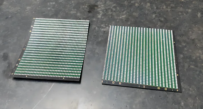
PCB warpage refers to the bending or twisting of a printed circuit board, resulting in an uneven or non-flat surface. This deformation can occur during manufacturing, assembly, or even after the board is in use. In SMT assembly, where precision is key, even a slight warp can cause major issues like misaligned components, poor solder joints, or complete assembly failures.
Warpage matters because it directly impacts the reliability and performance of electronic devices. For instance, during SMT reflow soldering, a warped board might prevent components from sitting flush on the surface, leading to defects such as tombstoning (where components stand upright on one end) or insufficient solder connections. According to industry standards like IPC-6012, the acceptable warpage for PCBs intended for SMT assembly is typically no more than 0.75% of the board's diagonal length. However, for high-density boards with miniaturized components, this tolerance often needs to be tighter, around 0.5% or less.
In this guide, we'll break down the root causes of warpage, align with IPC standards, and provide a warpage troubleshooting guide with best practices to ensure SMT success.
Common Causes of PCB Warpage in SMT Assembly
Understanding why PCB warpage happens is the first step to preventing it. Several factors during design, manufacturing, and assembly can contribute to this issue. Let’s explore the most common causes.
1. Uneven Copper Distribution
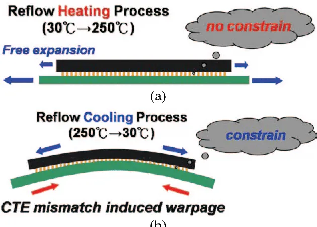
One of the leading causes of PCB warpage is an imbalance in copper distribution across the board’s layers. Copper expands and contracts with temperature changes during processes like reflow soldering. If one side or layer of the PCB has more copper than another, the uneven thermal expansion can cause the board to bend. For example, a board with heavy copper traces on one side and minimal copper on the other may warp by up to 1-2% under high temperatures (around 260°C during reflow).
2. Material Selection and Mismatch
The choice of materials for the PCB substrate and laminate can also lead to warpage. Different materials have varying coefficients of thermal expansion (CTE). If the CTE of the core material doesn’t match that of the copper or prepreg layers, stress builds up during thermal cycles, causing deformation. Standard FR-4 material, for instance, has a CTE of about 14-17 ppm/°C, while copper’s CTE is around 17 ppm/°C. A significant mismatch can exacerbate warpage risks.
3. Improper Manufacturing Processes
Manufacturing steps like lamination, curing, and etching can introduce warpage if not controlled properly. For instance, uneven pressure during lamination or inconsistent curing temperatures (often ranging from 150°C to 200°C) can create internal stresses in the board. These stresses may not be visible initially but can manifest as warpage during SMT reflow.
4. Thermal Stress During SMT Reflow
The high temperatures of SMT reflow soldering, often peaking at 240-260°C for lead-free solder, can aggravate existing stresses in the PCB. If the board isn’t designed to handle these thermal cycles, it may bow or twist. This is especially problematic for larger boards (over 12 inches in diagonal length) or thinner boards (less than 1.6 mm thick), where structural integrity is lower.
Related Reading: What is PCB Warpage?
PCB Warpage and IPC Standards: What You Need to Know
The IPC (Institute of Printed Circuits) sets industry standards to ensure quality and reliability in PCB manufacturing and assembly. When it comes to PCB warpage, the IPC-6012 standard for rigid PCBs specifies the maximum allowable bow and twist. As mentioned earlier, the general guideline is a warpage limit of 0.75% for SMT assembly boards. This means that for a board with a diagonal length of 10 inches, the maximum deviation from flatness should not exceed 0.075 inches.
For more advanced applications, such as high-density interconnect (HDI) boards with fine-pitch components, stricter tolerances may apply. IPC-A-610, which focuses on the acceptability of electronic assemblies, also emphasizes the importance of flatness during SMT processes to avoid assembly defects like open solder joints or component misalignment.
Adhering to these IPC standards is not just about compliance; it’s about ensuring that your boards perform reliably in real-world conditions. Manufacturers and designers must work together to meet these benchmarks through careful design and process control.
SMT Assembly Defects Caused by Warpage
Warpage doesn’t just affect the PCB itself; it creates a ripple effect of defects during SMT assembly. Here are some of the most common issues tied to "SMT assembly defects warpage."
1. Component Misalignment
When a PCB is warped, components may not sit flat on the surface during placement. This misalignment can prevent proper contact with solder paste, leading to weak or missing connections. For fine-pitch components like 0402 resistors or QFN packages, even a 0.1 mm deviation can cause assembly failures.
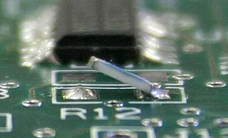
2. Tombstoning
Tombstoning occurs when one end of a component lifts off the board during reflow, resembling a tombstone. Warpage can exacerbate this by creating uneven heating or solder wetting across the board. This defect is particularly common with small chip components and can lead to open circuits.
3. Insufficient Solder Joints
A warped board may result in uneven solder paste application or poor contact between pads and components. This can cause insufficient solder joints, reducing the mechanical and electrical reliability of the assembly. Over time, these weak joints may fail under thermal or mechanical stress.
Warpage Troubleshooting Guide: Identifying and Fixing Issues
If you’re facing PCB warpage issues, a systematic approach can help you identify and resolve the problem. Follow this "warpage troubleshooting guide" to get back on track.
Step 1: Measure Warpage Accurately
Use a flatness measurement tool, such as a dial gauge or laser scanner, to quantify the extent of warpage. Compare the results against IPC-6012 standards (0.75% maximum for SMT boards). For a 10-inch board, this means the height difference between the highest and lowest points should not exceed 0.075 inches. Identifying the degree of warpage helps determine whether the issue is within acceptable limits or requires immediate action.
Step 2: Review Design for Copper Balance
Check the PCB layout for uneven copper distribution. If one layer has significantly more copper (e.g., large ground planes) than others, consider adding dummy copper fills or balancing the design to distribute copper evenly. Many design tools allow you to calculate copper density per layer to spot imbalances early.
Step 3: Evaluate Material and Stack-Up
Ensure that the materials used (e.g., FR-4, high-Tg laminates) have compatible CTE values. If mismatches are found, consult with your material supplier to select a better combination. Additionally, review the stack-up design to ensure symmetry, as asymmetrical stack-ups can contribute to warpage under thermal stress.
Step 4: Assess Manufacturing and Assembly Processes
Work with your manufacturing partner to verify that lamination pressures, curing temperatures, and reflow profiles are optimized. For instance, a gradual cooling phase after reflow (cooling at 2-3°C per second) can reduce thermal shock and minimize warpage. If warpage occurs post-reflow, consider using fixtures or carriers to hold the board flat during soldering.
Best Practices to Prevent PCB Warpage
Prevention is always better than correction. Incorporate these "best practices" into your design and manufacturing workflow to minimize PCB warpage and ensure SMT success.
1. Balance Copper Distribution in Design
During the design phase, aim for uniform copper distribution across all layers. If a layer has large empty areas, add dummy copper fills or mesh patterns to balance thermal expansion. Many PCB design tools provide copper density analysis to help achieve this balance.
2. Choose Compatible Materials
Select materials with matching CTE values for the substrate, copper, and prepreg layers. For high-temperature applications, consider high-Tg FR-4 or polyimide materials, which offer better thermal stability (Tg values of 170°C or higher compared to standard FR-4’s 130-140°C).
3. Optimize PCB Stack-Up
Design a symmetrical stack-up to reduce internal stresses. For example, in a 4-layer board, ensure that the top and bottom layers mirror each other in terms of copper thickness and placement. Symmetry helps the board expand and contract uniformly during thermal cycles.
Related Reading: Total PCB Thickness and Warpage issue
4. Control Reflow Profiles
During SMT assembly, use a well-optimized reflow profile with gradual heating and cooling rates. Avoid rapid temperature changes, as they can induce thermal shock. A typical lead-free reflow profile might include a preheat phase at 150-180°C for 60-90 seconds, a peak temperature of 245-260°C for 20-40 seconds, and a controlled cooling rate of 2-4°C per second.
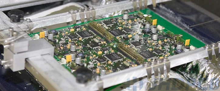
5. Use Support Fixtures for Larger Boards
For larger or thinner PCBs, use support fixtures or carriers during reflow to keep the board flat. These fixtures can prevent warpage by providing mechanical support under high temperatures. Ensure the fixture material can withstand reflow temperatures without deforming.
How Warpage Impacts Long-Term Reliability
Beyond immediate SMT assembly defects, PCB warpage can affect the long-term reliability of electronic products. Warped boards may experience increased mechanical stress on solder joints, leading to cracks or failures over time. Additionally, warpage can cause uneven thermal dissipation, creating hot spots that degrade components or reduce the lifespan of the device.
For critical applications, such as automotive or aerospace electronics, even minor warpage can compromise safety and performance. By addressing warpage early in the design and manufacturing stages, you can avoid these long-term risks and ensure consistent product quality.
Partnering for Success: How We Can Help
At ALLPCB, we understand the challenges of PCB warpage and its impact on SMT assembly. Our team is committed to providing high-quality manufacturing solutions tailored to your needs. From material selection to process optimization, we work closely with you to minimize warpage and achieve reliable results. With adherence to IPC standards and a focus on precision, we’re here to support your projects every step of the way.
Conclusion: Mastering PCB Warpage for SMT Excellence
PCB warpage is a complex issue, but with the right knowledge and strategies, it’s entirely manageable. By understanding the causes—such as uneven copper distribution, material mismatches, and thermal stress—you can take proactive steps to prevent it. Following IPC standards like IPC-6012 ensures your boards meet industry benchmarks, while our warpage troubleshooting guide and best practices offer practical solutions for SMT success.
Whether you’re a designer or manufacturer, tackling PCB warpage starts with careful planning and collaboration. Implement the tips in this guide, from balancing copper in design to optimizing reflow profiles, and watch your assembly yields improve. With these strategies, you’re well on your way to producing flat, reliable PCBs that stand up to the demands of modern electronics.


