 ALLPCB


If you're in the process of designing or manufacturing a printed circuit board (PCB), you've likely come across the terms ENIG and Gold Plating as surface finish options. But what’s the difference between ENIG vs Gold Plating for PCB boards? In short, ENIG (Electroless Nickel Immersion Gold) is a two-layer finish with a nickel base and a thin gold top layer applied through a chemical process, offering excellent flatness and solderability. Gold Plating, on the other hand, is an electroplated process that deposits a thicker layer of gold, often over a nickel base, and is typically used for applications requiring durability, like edge connectors.
In this detailed guide, we’ll dive deep into the specifics of ENIG and Gold Plating, comparing their processes, benefits, drawbacks, and ideal applications. Whether you're an engineer, designer, or procurement specialist, this blog will help you make an informed decision for your next PCB project.
What Are PCB Surface Finishes and Why Do They Matter?
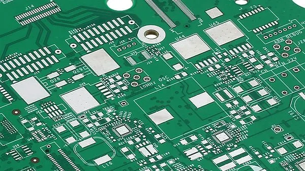
Before we explore the differences between ENIG and Gold Plating, let’s understand the role of surface finishes in PCB manufacturing. A surface finish is a protective coating applied to the exposed copper on a PCB to prevent oxidation, ensure solderability, and enhance the board’s performance and longevity. Without a proper finish, copper can corrode, leading to poor connections and potential failure of the board.
Surface finishes also impact how well components can be soldered to the board, the board’s ability to withstand environmental factors, and its suitability for specific applications. Choosing the right finish can affect everything from cost to reliability, making it a critical decision in PCB design.
What Is ENIG (Electroless Nickel Immersion Gold)?
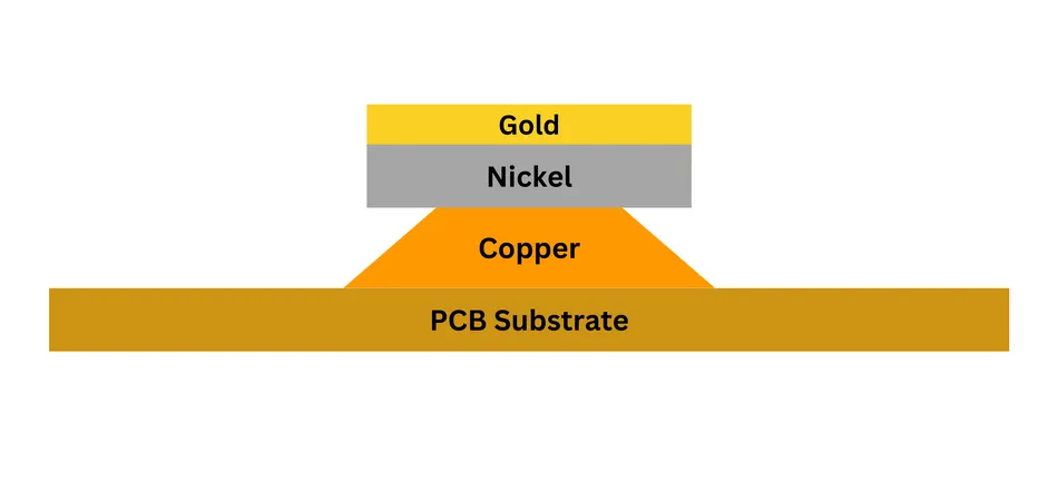
ENIG is a popular surface finish in PCB manufacturing due to its versatility and reliability. It consists of two layers: a base layer of nickel (typically 3-6 micrometers thick) and a thin top layer of gold (around 0.05-0.1 micrometers thick). The nickel acts as a barrier to prevent copper diffusion, while the gold protects the nickel from oxidation and ensures excellent solderability.
The process of applying ENIG is chemical, meaning it doesn’t require an electric current. The board is first coated with nickel through an electroless process, and then a thin layer of gold is deposited via immersion. This results in a very flat surface, which is ideal for fine-pitch components and surface-mount technology (SMT).
Key Benefits of ENIG
- Excellent Flatness: The uniform coating makes ENIG ideal for high-density designs with small components.
- Good Solderability: The gold layer ensures reliable soldering, even after prolonged storage.
- Corrosion Resistance: The nickel-gold combination provides strong protection against oxidation.
- Long Shelf Life: ENIG-finished boards can be stored for extended periods without degrading.
Drawbacks of ENIG
- Higher Cost: The process and materials used in ENIG make it more expensive than some other finishes.
- Black Pad Risk: If not applied correctly, a phenomenon called "black pad" can occur, where the nickel layer corrodes, leading to poor solder joints.
What Is Gold Plating for PCBs?
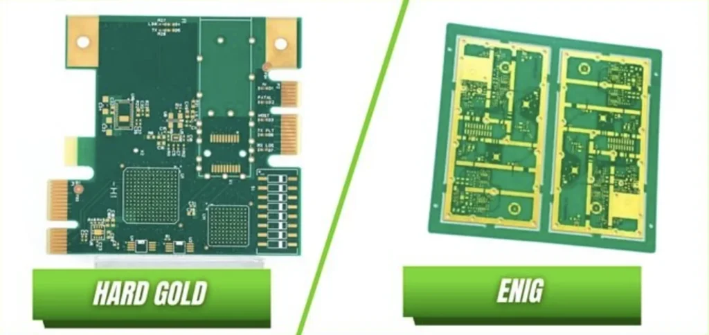
Gold Plating, often referred to as Hard Gold or Electroplated Gold, is another surface finish option for PCBs. Like ENIG, it typically involves a nickel underlayer (around 3-6 micrometers) topped with a layer of gold. However, the gold layer in Gold Plating is thicker, ranging from 0.25 to 1.25 micrometers or more, depending on the application.
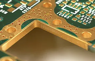
Unlike ENIG, Gold Plating uses an electroplating process, where an electric current is applied to deposit the gold onto the board. This method allows for a more controlled and thicker gold layer, making it suitable for applications that require high wear resistance, such as edge connectors on PCBs used in devices that are frequently plugged and unplugged.
Key Benefits of Gold Plating
- High Durability: The thicker gold layer withstands repeated mechanical stress, making it ideal for connectors.
- Excellent Conductivity: Gold Plating offers superior electrical conductivity, which is critical for high-performance applications.
- Customizable Thickness: The electroplating process allows for varying gold thicknesses based on specific needs.
Drawbacks of Gold Plating
- Poor Solderability: The thicker gold layer can lead to issues like gold embrittlement during soldering, where too much gold dissolves into the solder joint, weakening it.
- Higher Cost: Gold Plating is often more expensive than ENIG due to the thicker gold layer and the complexity of the process.
- Less Flatness: Compared to ENIG, Gold Plating may result in a less uniform surface, which can be problematic for fine-pitch components.
ENIG vs Gold Plating: A Detailed Comparison
Now that we’ve covered the basics of ENIG and Gold Plating, let’s compare them across several key factors to help you decide which finish is best for your PCB project.
1. Process and Application Method
ENIG uses a chemical immersion process, which results in a thin, uniform gold layer. This makes it a simpler and more consistent process for large-scale production. Gold Plating, however, relies on electroplating, which requires more precise control and is often applied selectively to specific areas like connectors.
2. Thickness of Gold Layer
The gold layer in ENIG is very thin (0.05-0.1 micrometers), while Gold Plating offers a thicker layer (0.25-1.25 micrometers or more). This difference impacts their durability and suitability for different applications. Thicker gold is better for high-wear areas, while thinner gold works well for soldering.
3. Solderability
ENIG excels in solderability due to its thin gold layer, which dissolves easily into the solder without causing embrittlement. Gold Plating, with its thicker gold layer, can lead to weaker solder joints if too much gold mixes with the solder, making it less ideal for SMT applications.
4. Durability and Wear Resistance
Gold Plating is the clear winner when it comes to durability. Its thicker gold layer can handle repeated mechanical stress, such as plugging and unplugging, without wearing down. ENIG, with its thinner gold layer, is less suited for such applications.
5. Flatness and Suitability for Fine-Pitch Components
ENIG provides a flatter surface, which is critical for high-density PCB designs with fine-pitch components. Gold Plating, due to the nature of the electroplating process, may result in slight unevenness, making it less ideal for such designs.
6. Cost Considerations
Both ENIG and Gold Plating are more expensive than other finishes like HASL (Hot Air Solder Leveling). However, Gold Plating tends to be costlier due to the thicker gold layer and the complexity of the electroplating process. For budget-conscious projects, ENIG might be the more economical choice unless durability is a priority.
When to Choose ENIG for Your PCB
ENIG is an excellent choice for a wide range of applications due to its balance of performance and reliability. Consider using ENIG if your project involves:
- High-density designs with fine-pitch components, such as smartphones or medical devices.
- Applications where solderability is critical, especially for surface-mount components.
- Boards that may need to be stored for long periods before assembly, as ENIG offers a long shelf life.
For example, in a PCB designed for a compact IoT device with components spaced less than 0.5 mm apart, ENIG’s flat surface ensures precise placement and reliable soldering.
When to Choose Gold Plating for Your PCB
Gold Plating is the go-to option for applications where durability and wear resistance are paramount. Opt for Gold Plating if your project includes:
- Edge connectors or areas subject to frequent mechanical stress, such as in memory cards or USB connectors.
- High-performance applications requiring excellent conductivity, like in aerospace or military equipment.
- Specific areas of the board that need a thicker gold layer for longevity.
For instance, in a PCB used in a rugged industrial control system where connectors are plugged and unplugged daily, Gold Plating ensures the connectors remain functional over thousands of cycles.
Other Factors to Consider in PCB Surface Finishes
Beyond the differences between ENIG and Gold Plating, there are other factors to keep in mind when selecting a surface finish for your PCB:
- Environmental Conditions: If your PCB will be exposed to harsh environments (e.g., high humidity or extreme temperatures), ensure the finish provides adequate protection against corrosion.
- Signal Integrity: For high-frequency applications, the surface finish can impact signal loss. Both ENIG and Gold Plating generally perform well, but Gold Plating’s superior conductivity might offer a slight edge.
- Manufacturing Capabilities: Not all manufacturers can apply these finishes with the same quality. Ensure your manufacturing partner has the expertise to avoid issues like black pad in ENIG or uneven coating in Gold Plating.
Conclusion: Making the Right Choice for Your PCB Project
Choosing between ENIG vs Gold Plating for your PCB board depends on your specific needs and application. If you prioritize flatness, solderability, and versatility for high-density designs, ENIG is likely the better choice. However, if your project requires exceptional durability for connectors or high conductivity for critical applications, Gold Plating is the way to go.
Understanding the strengths and limitations of each finish allows you to optimize your PCB for performance, reliability, and cost. By carefully considering factors like component spacing, mechanical stress, and environmental exposure, you can select the surface finish that best aligns with your project goals.


