ALLPCB


If you're dealing with PCB plating defects, you're not alone. These issues can lead to poor performance, unreliable circuits, and costly rework in manufacturing. Common PCB plating defects include uneven plating, pitting, blisters, and insufficient thickness, often caused by contamination, improper process control, or material issues. The good news? Most of these problems can be prevented with proper quality control, troubleshooting techniques, and optimized manufacturing practices. In this comprehensive guide, we'll dive deep into the causes of PCB plating defects, how to identify them, and actionable steps to prevent them, ensuring high-quality boards for your projects.
What Are PCB Plating Defects?
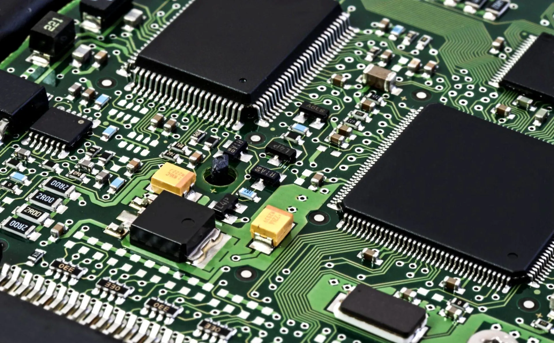
PCB plating is a critical step in the manufacturing process where a thin layer of metal, usually copper, nickel, or gold, is deposited onto the surface of a printed circuit board (PCB). This layer protects the board, enhances conductivity, and ensures proper soldering. However, defects in the plating process can compromise the board's functionality and durability. PCB plating defects refer to imperfections in this metal layer, such as cracks, uneven coverage, or weak adhesion, which can lead to electrical failures or physical damage over time.
Understanding and addressing these defects is essential for maintaining quality in PCB production. Whether you're an engineer, a manufacturer, or a hobbyist, recognizing the signs of plating issues early can save time and resources. Let's explore the most common types of PCB plating defects and their root causes.
Common Types of PCB Plating Defects
Plating defects can manifest in various forms, each with unique causes and effects on the board's performance. Below are some of the most frequent issues encountered during PCB manufacturing:
1. Uneven Plating Thickness
Uneven plating occurs when the metal layer is not uniformly deposited across the PCB surface. This can result in areas with insufficient protection or conductivity, leading to weak solder joints or signal integrity issues. For instance, if the copper layer in a high-frequency circuit varies from 1 oz/ft2 to 0.5 oz/ft2 across the board, it can disrupt impedance matching, often targeted at 50 ohms for standard designs.
Causes: Poor agitation during the plating bath, inconsistent current distribution, or improper cleaning before plating.
2. Pitting and Voids
Pitting appears as small holes or depressions in the plated layer, while voids are areas where no plating exists at all. These defects weaken the board's structure and can cause electrical shorts or corrosion over time. Pitting is often visible under magnification and can be as small as 0.1 mm in diameter, yet still impactful.
Causes: Contamination in the plating solution, trapped air bubbles, or inadequate surface preparation.
3. Blisters and Delamination
Blisters are raised areas in the plating caused by trapped gases or moisture, while delamination refers to the separation of the plated layer from the substrate. Both issues can lead to complete circuit failure, especially in harsh environments where thermal expansion (e.g., from -40°C to 85°C) stresses the board.
Causes: Moisture trapped in the substrate, poor adhesion due to surface contaminants, or excessive plating stress.
4. Insufficient Plating Thickness
If the plated layer is too thin, it may not provide adequate protection or conductivity. Industry standards often require a minimum copper thickness of 25 micrometers (1 mil) for through-hole components. Falling below this can lead to reliability issues during soldering or operation.
Causes: Incorrect plating time, low current density, or depleted plating solution.
5. Cracks in Plating
Cracks in the plated layer can expose the underlying material to corrosion and create points of failure in the circuit. These are often seen in boards subjected to mechanical stress or thermal cycling, where temperature fluctuations exceed 100°C.
Causes: Excessive internal stress in the plating, improper cooling after plating, or material mismatch.
Root Causes of PCB Plating Defects
To prevent plating defects, it's crucial to understand their underlying causes. Many of these issues stem from controllable factors in the manufacturing process. Let's break down the primary reasons for plating problems:
1. Contamination in Materials or Solutions
Contaminants such as dust, oil, or organic residues on the PCB surface or in the plating bath can interfere with metal deposition. Even trace amounts of impurities, as low as 1 ppm, in the plating solution can cause pitting or uneven layers.
2. Poor Surface Preparation
Before plating, the PCB surface must be thoroughly cleaned and activated. If residues from etching or drilling remain, they can prevent proper adhesion of the plated layer, leading to blisters or delamination.
3. Improper Plating Parameters
Plating requires precise control of parameters like current density, temperature, and bath agitation. For example, a current density outside the optimal range of 2-4 A/dm2 for copper plating can result in uneven thickness or burns on the board.
4. Material Incompatibility
Using substrates or plating materials that are not compatible can lead to adhesion issues. For instance, a mismatch in thermal expansion coefficients between the substrate and plating metal can cause cracks during temperature changes.
5. Environmental Factors
High humidity or temperature fluctuations in the manufacturing environment can introduce moisture into the process, leading to defects like blisters. Maintaining a controlled environment with humidity below 50% is often recommended.
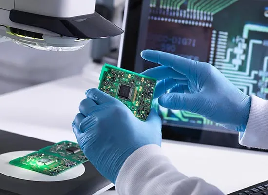
How to Identify PCB Plating Defects
Early detection of plating defects can prevent costly failures down the line. Here are some practical methods for identifying issues during and after the manufacturing process:
1. Visual Inspection
A simple visual check under good lighting can reveal obvious defects like blisters, uneven plating, or discoloration. Using a magnifying glass or microscope can help spot smaller issues like pitting, often as tiny as 0.05 mm in size.
2. Automated Optical Inspection (AOI)
AOI systems use cameras and software to scan PCBs for surface defects. These systems can detect inconsistencies in plating thickness or voids with high precision, often within tolerances of 0.01 mm.
3. Cross-Sectional Analysis
Cutting a sample of the PCB and examining it under a microscope allows for detailed inspection of plating thickness and adhesion. This method can confirm if the copper layer meets the required 25-35 micrometers for standard boards.
4. Electrical Testing
Testing the board for continuity and resistance can indirectly reveal plating defects. For instance, a higher-than-expected resistance (above 10 milliohms) in a trace might indicate insufficient plating thickness.
Preventing PCB Plating Defects: Best Practices
Preventing plating defects requires a proactive approach to quality control and process optimization. By addressing the root causes, manufacturers can significantly reduce the occurrence of these issues. Here are actionable strategies to ensure high-quality plating:
1. Optimize Surface Preparation
Ensure thorough cleaning and activation of the PCB surface before plating. Use chemical cleaners to remove oils and residues, and micro-etch the surface to improve adhesion. A clean surface reduces the risk of voids and blisters by up to 80%, based on industry observations.
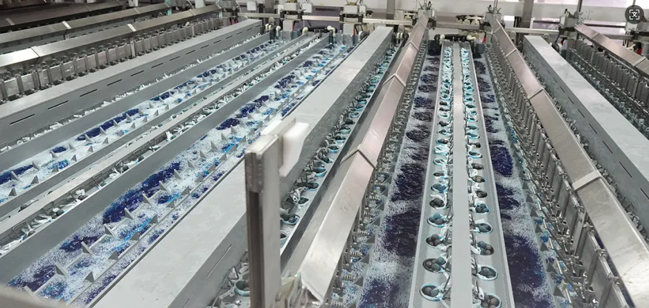
2. Maintain Plating Bath Quality
Regularly monitor and filter the plating solution to remove contaminants. Keep chemical concentrations within specified limits, and replace the bath when additives break down. For copper plating, maintain a sulfuric acid concentration of 180-220 g/L for optimal results.
3. Control Plating Parameters
Set and monitor current density, temperature, and agitation during plating. For example, maintain a bath temperature of 20-30°C for copper plating to avoid stress in the deposited layer. Use automated systems to ensure consistency across batches.
4. Use High-Quality Materials
Select substrates and plating materials that are compatible and meet industry standards. Avoid low-grade laminates that may absorb moisture, and use high-purity metals for plating to minimize defects.
5. Implement Strict Quality Control
Incorporate multiple inspection points in the manufacturing process. Conduct visual and automated inspections after each plating stage to catch defects early. Statistical process control (SPC) can help track variations and maintain a defect rate below 1%.
6. Train Staff and Standardize Procedures
Ensure that all personnel involved in PCB manufacturing are trained in proper handling and process execution. Standard operating procedures (SOPs) should be documented and followed to minimize human error.
Troubleshooting PCB Plating Defects
Even with preventive measures, defects can still occur. When they do, a systematic troubleshooting approach can help identify and resolve the issue. Follow these steps to address plating problems:
1. Analyze the Defect Type
Determine the specific defect (e.g., pitting, uneven thickness) through visual or microscopic inspection. Document the location and extent of the issue for further analysis.
2. Review Process Parameters
Check the plating parameters used during production, such as current density and bath temperature. Compare them against recommended values to identify deviations. For instance, a current density above 5 A/dm2 might explain burns or cracks.
3. Inspect Raw Materials
Examine the PCB substrate and plating solution for contamination or quality issues. Test the solution's chemical composition to ensure it meets specifications.
4. Adjust and Retest
Make necessary adjustments to the process, such as increasing cleaning time or adjusting current settings. Run a small batch of boards under the revised conditions and inspect for improvements.
The Importance of Quality Control in PCB Manufacturing
Quality control is the backbone of reliable PCB production. By integrating robust inspection and testing protocols, manufacturers can minimize plating defects and ensure consistent performance. A defect rate as low as 0.5% can still impact thousands of boards in high-volume production, making stringent quality measures non-negotiable.
Investing in advanced inspection tools like AOI and X-ray systems can detect issues that are invisible to the naked eye. Additionally, adhering to industry standards such as IPC-A-600 for PCB acceptability ensures that plating meets the required thickness and adhesion criteria.
Conclusion
PCB plating defects can be a significant hurdle in achieving reliable and high-performing circuit boards, but they are largely preventable with the right approach. By understanding common issues like uneven plating, pitting, and blisters, and addressing their root causes through optimized processes and strict quality control, manufacturers can ensure superior board quality. Implementing best practices such as thorough surface preparation, precise control of plating parameters, and regular inspections can drastically reduce defect rates and improve overall production efficiency.
At ALLPCB, we are committed to delivering top-notch PCB manufacturing solutions by prioritizing quality at every step. Whether you're troubleshooting existing plating issues or looking to prevent them in future projects, these strategies can help you achieve durable and reliable boards for any application.