 ALLPCB


If you've ever encountered PCB failures—like intermittent connections, weak solder joints, or even total circuit failure—chances are you've come across the notorious Black Pad Phenomenon. This defect, most commonly associated with ENIG (Electroless Nickel Immersion Gold) surface finishes, can lead to costly rework, field returns, and compromised product reliability.
In this article, we'll explain what the black pad defect is, its root causes, its damaging effects, and—most importantly—how partnering with a manufacturer with rigorous process controls, like ALLPCB, can help you prevent it.
What Is the Black Pad Defect?
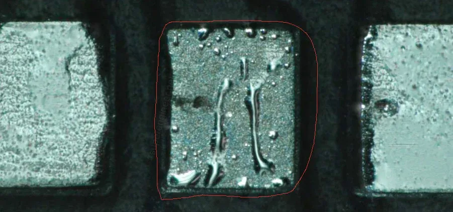
The black pad defect is a solderability failure mode in PCB manufacturing that results in a non-wettable, dark-colored pad surface. Instead of exhibiting the typical bright gold appearance expected of ENIG, affected pads appear dull, grainy, or even black.
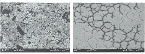
Microscopically, this darkened surface is a phosphorus-rich, brittle layer that forms in the nickel during the ENIG process. IPC-4552 (the industry specification for ENIG) defines this as nickel corrosion and classifies it into levels based on severity and depth. Under 1000× magnification, corrosion manifests as 'spikes,' 'spreader spikes,' or a 'black band' at the nickel–gold interface. Level-3 corrosion, as defined by IPC-4552A, is considered rejectable for Class 3 high-reliability products.
This corrosion prevents proper metallurgical bonding during soldering, leading to:
- Solder Rejection: Molten solder fails to wet the pad, beading up like water on a lotus leaf.
- Non-wetting Joints: Mechanically fragile joints that may fail under vibration or thermal cycling.
- Insufficient Fillets: Most solder is drawn onto component leads, leaving pads partially unbonded.
Consequences for PCB Performance and Reliability
The impact of black pad goes beyond assembly challenges—it affects the electrical and mechanical reliability of the entire product.
Electrical & Functional Impacts
- Open Circuits: Complete loss of continuity from fractured solder joints.
- Intermittent Faults: Hard-to-trace failures that appear only under thermal or mechanical stress.
- Signal Integrity Issues: Impedance discontinuities and reflections in high-speed designs.
Assembly & Mechanical Risks
- Poor Wetting: Leads to incomplete solder fillets.
- Voiding & Cracking: Brittle interfaces prone to crack propagation under stress.
- Thermal Fatigue: Accelerated joint degradation during normal operating cycles.

These risks are critical for automotive, aerospace, and medical electronics, where reliability is non-negotiable.
Why Black Pad Happens
The phenomenon is primarily linked to nickel over-corrosion during ENIG plating. Key contributing factors include:
- Excessive Nickel Etch: Overly aggressive immersion gold bath chemistry (high temperature, concentration, or dwell time).
- Bath Aging & Contamination: Accumulated by-products lead to nickel layers with out-of-spec phosphorus content (>11%). IPC-4552 specifies an optimal 7–11% range for electroless nickel phosphorus content to ensure corrosion resistance.
- Inadequate Rinsing: Cross-contamination between plating steps causes localized corrosion.
- Storage Conditions: Long-term exposure to humid environments prior to assembly accelerates oxidation.

IPC Requirements: What the Standards Say
IPC-4552B sets the following key parameters for ENIG finish:
- Nickel Thickness: 3–6 µm (118–236 µin)
- Gold Thickness: 0.04–0.10 µm (1.6–4.0 µin)
- Nickel Phosphorus Content: 7–11% (to avoid brittleness and corrosion susceptibility)
- Accept/Reject Criteria: Level 3 nickel corrosion (deep, widespread black banding or spike formation) is not acceptable for Class 2 or Class 3 boards.
By adhering to these process windows, manufacturers can dramatically reduce the risk of black pad formation.
How ALLPCB Prevents Black Pad Defects
At ALLPCB, we take a process-control-first approach to ENIG plating. Our quality system is aligned with IPC-4552B guidelines and includes:
Electroless Nickel Process Control
- Continuous Bath Monitoring: Real-time pH, temperature, and nickel ion concentration tracking.
- Impurity Control: Routine analysis to keep Cu, Pb, S contamination below IPC-defined limits.
- Phosphorus Content Management: Optimized chemistry maintains 7–10% P for maximum corrosion resistance.
- Predictive Maintenance: Bath replacement based on real-time performance data, not just calendar intervals.
Immersion Gold Process Optimization
- Controlled Etch Rate: Gold deposition time precisely tuned to activate the nickel surface without over-etching.
- Concentration Stability: Automated dosing keeps gold concentration within ±5% of target.

Comprehensive Chemical Management
- Filtration & Rinsing: Multi-stage counter-current rinsing to eliminate drag-out and cross-contamination.
- Regular Tank Turnover: Ensures fresh chemistry and consistent plating quality.
Tips for Designers & Buyers to Reduce Risk
While process control is the manufacturer's responsibility, design and sourcing choices matter too:
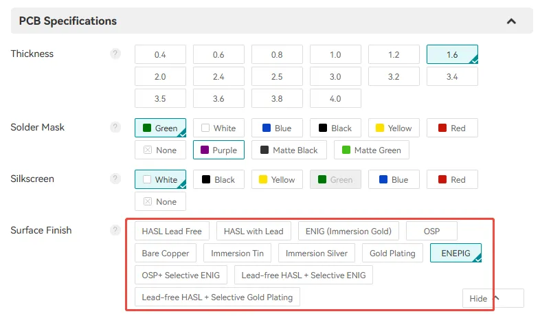
- Consider ENEPIG: For high-reliability designs, ENEPIG (Electroless Nickel Electroless Palladium Immersion Gold) provides an extra palladium barrier that virtually eliminates nickel corrosion. ALLPCB offers a wide range of surface treatment processes to help you choose the most suitable surface treatment for your products.
- Specify IPC-Class Compliance: Request IPC-6012 Class 3 fabrication and IPC-4552B ENIG compliance for mission-critical boards.
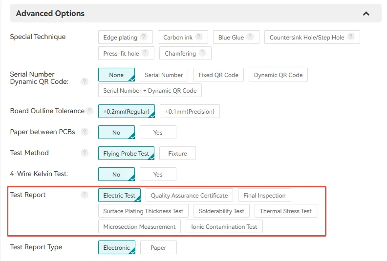
- Request Solderability Testing: Ask for solderability Test or microsection analysis prior to shipment for additional assurance.
- Select Experienced Suppliers: Partner with manufacturers with proven chemical control systems and IPC certification—like ALLPCB.
Conclusion
Black pad is a well-known but avoidable defect. By understanding its causes and aligning with IPC-4552B process controls, you can minimize risk and ensure long-term product reliability. At ALLPCB, we combine real-time process monitoring, predictive analytics, and strict quality control to deliver ENIG finishes with outstanding solderability and reliability—helping you build products that perform flawlessly in the field.


