 ALLPCB


In the fast-evolving world of automotive technology, Advanced Driver Assistance Systems (ADAS) are at the forefront, making vehicles safer and smarter. These systems rely heavily on compact, high-performance electronics, which in turn depend on High-Density Interconnect (HDI) Printed Circuit Boards (PCBs). If you're an engineer or designer looking to optimize HDI PCB stack-up strategies for compact ADAS modules, you're in the right place. This blog dives deep into HDI PCB microvia design, ADAS PCB layer stackup, high-density interconnect PCB techniques, blind and buried vias in ADAS PCBs, and HDI PCB design rules for automotive applications. We'll provide actionable insights to help you design efficient, reliable, and compact boards for automotive systems.
Let’s explore how HDI PCB stack-up strategies can address the unique challenges of ADAS modules, ensuring high performance in limited space while meeting stringent automotive standards.
Why HDI PCBs Are Essential for ADAS Modules
ADAS modules, such as radar, LiDAR, cameras, and ultrasonic sensors, require PCBs that can handle complex circuits in a small footprint. Traditional PCBs often fall short due to their larger size and limited routing capabilities. This is where HDI PCBs shine. With their ability to pack more components into a smaller area using advanced techniques like microvias and multiple layers, HDI PCBs are the go-to choice for compact, high-performance automotive designs.
HDI technology offers several advantages for ADAS applications:
- Compact Design: HDI PCBs reduce board size by up to 60%, allowing for smaller ADAS modules that fit into tight vehicle spaces.
- Improved Signal Integrity: Shorter signal paths and reduced noise ensure reliable data transmission, critical for real-time ADAS functions like collision detection.
- Higher Reliability: HDI boards use advanced materials and structures that withstand the harsh automotive environment, including temperature swings from -40°C to 85°C and vibrations up to 10G.
Now, let’s break down the key strategies for designing HDI PCB stack-ups tailored for ADAS modules.
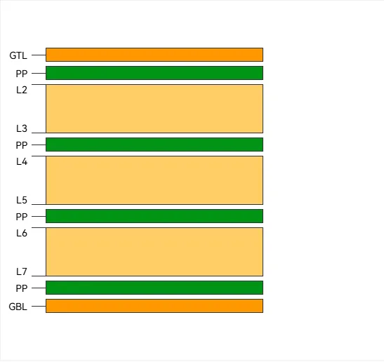
Understanding HDI PCB Stack-Up for ADAS Modules
An HDI PCB stack-up refers to the arrangement of conductive and insulating layers in a board, along with the vias that connect them. For ADAS modules, the stack-up must balance compactness, signal integrity, and manufacturability. A well-planned ADAS PCB layer stackup minimizes electromagnetic interference (EMI), supports high-speed signals (often exceeding 1 GHz for radar systems), and ensures thermal stability.
Common HDI stack-up structures for ADAS include:
- Sequential Build-Up (SBU): Layers are added sequentially with microvias connecting them, ideal for 6- to 10-layer boards in compact designs.
- Every Layer Interconnect (ELIC): Every layer is interconnected with microvias, allowing for maximum density in 12+ layer boards used in complex ADAS systems.
Key Considerations for ADAS PCB Layer Stackup
When designing the stack-up for ADAS modules, consider the following:
- Layer Count: ADAS boards often require 6 to 12 layers to accommodate high-speed signals, power distribution, and ground planes. For instance, a radar module might use an 8-layer stack-up with dedicated layers for signal routing and EMI shielding.
- Material Selection: Use high-Tg (glass transition temperature) materials like FR-4 or polyimide to handle automotive temperature ranges. A Tg of 170°C or higher is recommended for reliability.
- Ground and Power Planes: Place continuous ground planes adjacent to signal layers to reduce EMI and maintain impedance control, targeting values like 50 ohms for high-speed differential pairs.
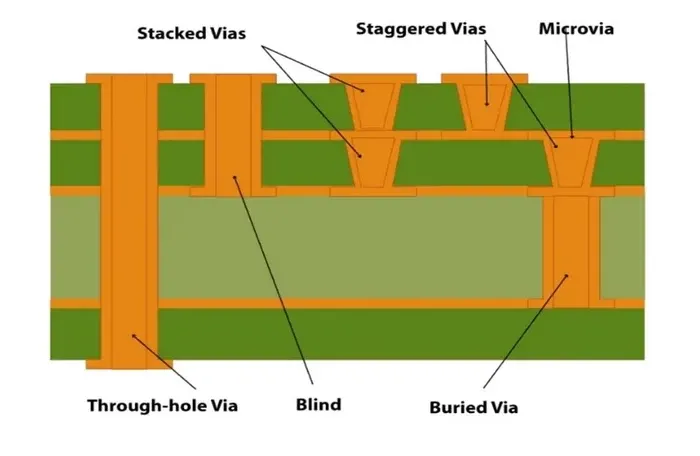
HDI PCB Microvia Design: Precision for Compactness
Microvias are tiny holes (typically less than 0.15 mm in diameter) used in HDI PCBs to connect layers without occupying much space. In ADAS modules, HDI PCB microvia design is critical for achieving high-density routing while maintaining signal integrity and reliability under automotive conditions.
Types of Microvias in HDI PCBs
- Blind Vias: These connect an outer layer to an inner layer without going through the entire board, saving space and improving routing flexibility.
- Buried Vias: Located entirely within inner layers, these vias free up surface space for components, crucial for compact ADAS designs.
- Stacked Vias: Multiple microvias stacked on top of each other to connect several layers, often used in ELIC stack-ups for maximum density.
- Staggered Vias: Offset microvias that connect layers without stacking directly, offering a balance between density and manufacturability.
Design Tips for Microvias in ADAS PCBs
To ensure reliability and performance, follow these tips for microvia design:
- Aspect Ratio: Maintain a microvia aspect ratio (depth-to-diameter) of 0.75:1 or less to ensure reliable plating and avoid failures. For a 0.1 mm diameter via, the depth should not exceed 0.075 mm.
- Pad Size: Use a capture pad at least 0.1 mm larger than the via diameter to ensure proper alignment during manufacturing.
- Thermal Cycling: Design microvias to withstand thermal expansion in automotive environments. Use laser-drilled microvias for precision and durability.
Leveraging Blind and Buried Vias in ADAS PCBs
Blind and buried vias in ADAS PCBs are game-changers for achieving high-density designs. These vias allow for more routing channels without increasing board size, which is vital for compact modules like camera systems or sensor hubs.
Benefits of Blind and Buried Vias
- Space Efficiency: By eliminating through-hole vias, blind and buried vias free up surface area for additional components or routing.
- Signal Integrity: Shorter via lengths reduce signal loss and crosstalk, critical for high-speed ADAS signals operating at frequencies up to 5 GHz.
- Reduced Layer Count: These vias can reduce the number of layers needed, lowering costs while maintaining performance.
Challenges and Solutions
While beneficial, blind and buried vias come with manufacturing challenges. They require precise drilling and plating processes, increasing production complexity. To mitigate this, collaborate closely with your PCB fabricator to ensure design rules align with their capabilities. For instance, specify a minimum via drill size of 0.1 mm for blind vias to avoid manufacturing defects.
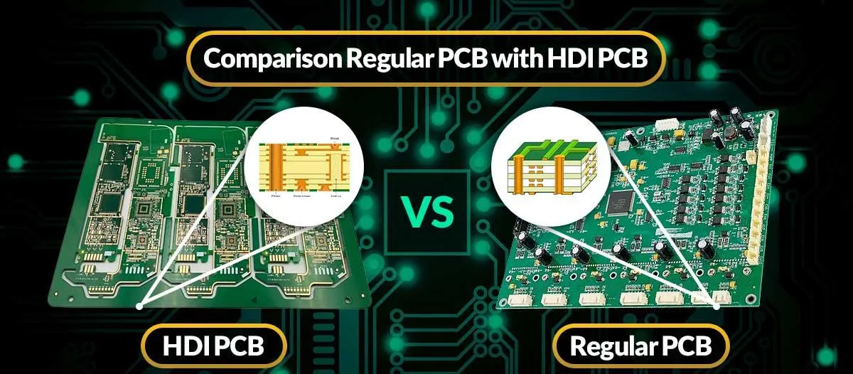
High-Density Interconnect PCB Techniques for ADAS
A high-density interconnect PCB is defined by its ability to support finer lines, smaller vias, and tighter spacing compared to standard boards. For ADAS modules, HDI techniques enable the integration of complex circuits, such as microcontrollers, sensors, and communication interfaces, into a single compact board.
Key HDI Techniques for ADAS
- Fine Line Width and Spacing: Use trace widths as narrow as 0.075 mm and spacing of 0.075 mm to maximize routing density. This allows for more connections in a smaller area.
- Via-in-Pad Design: Place vias directly under component pads to save space and shorten signal paths, improving performance for high-speed signals.
- Advanced Materials: Incorporate low-loss dielectrics with a dissipation factor (Df) of 0.005 or less to support high-frequency signals in radar and LiDAR systems.
HDI PCB Design Rules for Automotive Applications
Designing HDI PCBs for ADAS requires adherence to strict HDI PCB design rules for automotive standards to ensure reliability, safety, and compliance with regulations like ISO 26262 for functional safety.
Essential Design Rules
- Trace and Via Clearance: Maintain a minimum clearance of 0.1 mm between traces and vias to prevent short circuits, especially under high-voltage conditions in automotive systems.
- Impedance Control: Design differential pairs with controlled impedance (e.g., 100 ohms ±10%) to ensure consistent signal integrity for high-speed data transmission.
- Thermal Management: Incorporate thermal vias and copper pours to dissipate heat from high-power components, targeting a thermal resistance of less than 10°C/W.
- Automotive Standards Compliance: Ensure the design meets AEC-Q100 standards for stress testing, guaranteeing reliability under extreme conditions like humidity up to 85% RH.
Testing and Validation
Before production, simulate the PCB design using tools to analyze signal integrity, EMI, and thermal performance. Conduct environmental stress tests to validate the board’s durability under automotive conditions, such as thermal cycling between -40°C and 125°C for 1000 cycles.
Conclusion: Building Better ADAS Modules with HDI PCBs
HDI PCB stack-up strategies are the backbone of compact, high-performance ADAS modules. By focusing on HDI PCB microvia design, optimizing ADAS PCB layer stackup, leveraging high-density interconnect PCB techniques, utilizing blind and buried vias in ADAS PCBs, and adhering to HDI PCB design rules for automotive applications, engineers can create reliable and efficient designs that meet the demands of modern vehicles.
At ALLPCB, we’re committed to supporting your journey in designing cutting-edge HDI PCBs for automotive applications. Whether you’re working on radar systems, camera modules, or sensor hubs, applying these strategies will help you achieve compactness without compromising on performance or reliability. Start integrating these principles into your next ADAS project to stay ahead in the automotive innovation race.


