 ALLPCB


In the fast-growing world of renewable energy, printed circuit boards (PCBs) are at the heart of technologies like solar panels, wind turbines, and energy storage systems. Scaling up from a PCB prototype to mass production is a critical step for manufacturers aiming to meet the rising demand for clean energy solutions. This blog post explores the journey of PCB manufacturing scale up in the renewable energy sector, diving into the renewable energy PCB production process, PCB mass production strategies, and the detailed PCB manufacturing process from prototype to full-scale output.
Whether you're an engineer, a project manager, or a business owner in the renewable energy field, this guide will walk you through the essential steps, challenges, and best practices for transitioning from a PCB prototype to large-scale production. Let's dive into the details of how to make this process smooth, efficient, and cost-effective.
Why Renewable Energy PCB Manufacturing Is Crucial
The renewable energy sector is booming, with global investments reaching over $500 billion annually in recent years, according to industry reports. PCBs play a vital role in this growth, serving as the backbone of control systems, inverters, and battery management systems in solar, wind, and electric vehicle applications. As demand for these technologies surges, manufacturers must scale up production to keep pace.
Scaling renewable energy PCB production is not just about making more boards; it's about ensuring reliability, efficiency, and sustainability. A well-designed PCB can handle high voltages (often exceeding 600V in solar inverters) and maintain signal integrity at frequencies up to 100 MHz in advanced energy systems. Getting from a prototype to mass production requires precision at every stage to meet these demanding specifications.
Step 1: Perfecting the PCB Prototype
Before any PCB manufacturing scale up can happen, the prototype phase sets the foundation. A PCB prototype is a small-scale version of the final board, used to test design concepts, functionality, and performance. For renewable energy applications, prototypes must be rigorously tested under real-world conditions, such as temperature extremes (-40°C to 85°C) and high humidity levels (up to 85% RH), to ensure durability.
During this stage, focus on:
- Design Optimization: Use simulation tools to check for signal integrity and thermal performance. For example, ensure trace widths are sufficient to handle currents up to 10A in power conversion circuits.
- Material Selection: Choose materials like FR-4 or high-frequency laminates that can withstand the environmental stresses of renewable energy systems.
- Testing: Perform electrical tests to verify impedance values (typically targeting 50 ohms for high-speed signals) and mechanical tests for structural integrity.
Prototyping is also the time to identify potential issues that could become costly during PCB mass production. A single design flaw, like improper spacing between components, can lead to short circuits or signal interference, delaying production timelines.
Step 2: Transitioning from Prototype to Small Batch Production
Once the prototype is validated, the next step in the PCB manufacturing process is small batch production. This phase acts as a bridge between prototyping and full-scale PCB mass production. Small batches, often ranging from 50 to 500 units, allow manufacturers to test production processes and refine assembly techniques without the high costs of large-scale runs.
Key considerations during this stage include:
- Design for Manufacturability (DFM): Adjust the PCB layout to simplify assembly. For instance, ensure component placement allows for automated pick-and-place machines, reducing manual labor costs.
- Supplier Coordination: Secure reliable suppliers for components like MOSFETs and capacitors, which are critical for renewable energy PCBs and often have lead times of 8-12 weeks.
- Quality Control: Implement automated optical inspection (AOI) to detect defects like misaligned components or soldering issues, ensuring a defect rate below 1%.
This stage also helps identify bottlenecks in the production line, such as slow etching processes or delays in component sourcing, which can be addressed before scaling up.
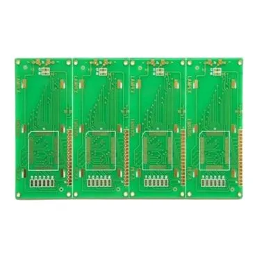
Step 3: Scaling Up to PCB Mass Production
Scaling up to PCB mass production is where the real challenges of PCB manufacturing scale up come into play. Producing thousands or even millions of units requires a streamlined process, significant investment in equipment, and strict quality assurance protocols. For renewable energy applications, where reliability is non-negotiable, the stakes are even higher.
Here are the critical steps for successful mass production:
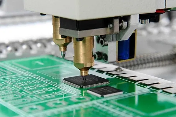
- Invest in Advanced Equipment: High-speed drilling machines and multi-layer lamination presses can increase output to over 10,000 boards per day while maintaining precision (drill accuracy within 0.1mm).
- Standardize Processes: Develop standardized operating procedures (SOPs) for every stage, from copper etching to final assembly, to ensure consistency across batches.
- Implement Robust Testing: Use in-circuit testing (ICT) to verify electrical performance and functional testing to simulate real-world conditions. Aim for a failure rate of less than 0.5% in production runs.
- Optimize Supply Chain: Establish long-term contracts with material suppliers to avoid shortages, especially for high-demand items like high-voltage capacitors.
Scaling up also means balancing cost and quality. While it's tempting to cut corners to reduce expenses, a single faulty batch of PCBs in a solar inverter system could lead to failures costing millions in repairs and lost trust.
Challenges in Renewable Energy PCB Production Scale Up
The journey of renewable energy PCB production from prototype to mass production is not without hurdles. Understanding these challenges can help manufacturers prepare and adapt.
- High Material Costs: Specialized materials for high-power applications, such as metal-core PCBs for thermal management, can cost up to 30% more than standard materials.
- Complex Designs: Renewable energy PCBs often require multi-layer designs (8-16 layers) to handle complex circuitry, increasing production time and error risks.
- Regulatory Compliance: Boards must meet strict standards like RoHS for environmental safety and IPC-6012 for performance, requiring additional testing and documentation.
- Environmental Impact: Manufacturing at scale consumes significant energy and resources. Adopting eco-friendly practices, like using recyclable materials, can reduce the carbon footprint but may increase upfront costs.
Addressing these challenges requires a proactive approach, such as investing in sustainable manufacturing technologies and building strong partnerships with supply chain stakeholders.
Best Practices for a Smooth PCB Manufacturing Process
To ensure a successful PCB manufacturing process when scaling up, consider these best practices tailored for renewable energy applications:
- Collaborate Early: Work closely with design engineers and production teams during the prototype phase to catch issues before they escalate in mass production.
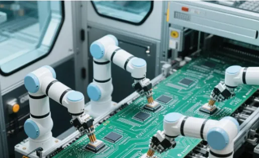
- Prioritize Automation: Automated assembly and testing systems can reduce human error and increase throughput by up to 40%, based on industry benchmarks.
- Focus on Sustainability: Use lead-free soldering and biodegradable packaging to align with the green ethos of renewable energy while meeting regulatory requirements.
- Monitor Performance Metrics: Track key performance indicators (KPIs) like yield rate (targeting above 98%) and cycle time (aiming for under 24 hours per batch) to identify areas for improvement.
By following these practices, manufacturers can minimize delays, reduce costs, and deliver high-quality PCBs that power the future of renewable energy.
The Role of Technology in Scaling PCB Production
Technology is a game-changer in the PCB manufacturing scale up process. Advanced tools and software streamline every aspect of production, from design to delivery.
- CAD Software: Modern computer-aided design tools allow for precise modeling of complex renewable energy PCBs, reducing design errors by up to 50%.
- IoT Integration: Internet of Things (IoT) systems in smart factories enable real-time monitoring of production lines, cutting downtime by 20-30%.
- AI for Quality Control: Artificial intelligence algorithms can predict defects before they occur, achieving accuracy rates above 95% in defect detection.
Embracing these technologies not only boosts efficiency but also positions manufacturers as leaders in the competitive renewable energy market.
Conclusion: Building a Sustainable Future with Renewable Energy PCBs
Scaling up renewable energy PCB production from a PCB prototype to PCB mass production is a complex but rewarding journey. By focusing on design optimization, rigorous testing, and streamlined manufacturing processes, companies can meet the growing demand for clean energy solutions while maintaining quality and reliability.
The PCB manufacturing scale up process requires careful planning, investment in technology, and a commitment to sustainability. As the renewable energy sector continues to expand, manufacturers who master this transition will play a pivotal role in powering a greener future.
At ALLPCB, we're dedicated to supporting this mission by providing end-to-end solutions for PCB design, prototyping, and production. Whether you're at the prototype stage or ready to scale up, our expertise ensures your renewable energy projects succeed at every step of the PCB manufacturing process.


