 ALLPCB


Designing a circuit board layout can be a rewarding yet challenging task for electric hobbyists. Whether you're building a simple project or a complex electronic device, a well-thought-out printed circuit board (PCB) design ensures functionality, reliability, and ease of assembly. In this guide, we'll share practical tips to help you create an effective circuit board layout, with a focus on choosing the right PCB material and understanding board fabrication notes. Let's dive into the essentials of PCB design tailored for hobbyists, so you can bring your ideas to life with confidence.
Why a Good Circuit Board Layout Matters for Hobbyists
A proper circuit board layout is the backbone of any electronic project. It determines how components connect, how signals flow, and how well your device performs. For electric hobbyists, a good layout can mean the difference between a working prototype and a frustrating pile of errors. Issues like signal interference, overheating, or poor component placement can ruin a project. By following best practices, you can avoid common pitfalls and create a board that works as intended. Plus, understanding aspects like PCB material selection and board fab notes can save you time and money during manufacturing.
Tip 1: Start with a Clear Schematic
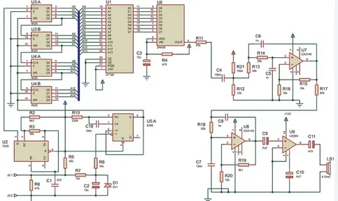
Before you even think about laying out your circuit board, you need a solid schematic. This is like a blueprint for your PCB, showing how every component connects electrically. As a hobbyist, take the time to double-check your schematic for errors. A small mistake here can lead to big problems on the board. Use design software to create and verify your schematic. Ensure that every connection is accurate and that you've accounted for power supply requirements, such as voltage levels (e.g., 5V or 12V) and current needs.
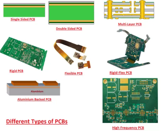
Tip 2: Choose the Right PCB Material
Selecting the appropriate PCB material is crucial for the performance and durability of your circuit board. The most common material for hobbyist projects is FR-4, a fiberglass epoxy laminate that offers a good balance of cost, strength, and electrical insulation. FR-4 is suitable for most low-to-medium frequency applications, with a dielectric constant of around 4.5, which helps maintain signal integrity up to a few hundred MHz.
For projects involving high temperatures or high-frequency signals (above 1 GHz), you might consider materials like Rogers or Teflon-based laminates. However, these are more expensive and often unnecessary for typical hobbyist projects like LED circuits or simple microcontrollers. Also, think about the thickness of the PCB material—standard thicknesses are 1.6mm or 0.8mm. Thinner boards are lighter and cheaper but may be less durable. Match the material to your project's needs to avoid overpaying or underperforming.
Tip 3: Plan Your Component Placement
Once your schematic is ready, it's time to place components on the board. Start by grouping related components together. For example, keep power supply components like voltage regulators and capacitors near each other to minimize noise. Place sensitive components, like analog sensors, away from noisy digital circuits to reduce interference.
Pay attention to the orientation of components. For surface-mount devices (SMD), align them in the same direction to make soldering easier and reduce errors during assembly. Also, ensure there's enough space between components for heat dissipation—overcrowding can lead to overheating. As a rule of thumb, leave at least 0.5mm of clearance between smaller components and 1-2mm for larger ones like electrolytic capacitors.
Tip 4: Optimize Trace Routing for Signal Integrity
Routing traces is where many hobbyists struggle, but it’s a critical step in PCB design. Traces are the copper paths that connect components, and their layout affects signal quality and power delivery. Keep traces as short and direct as possible to minimize resistance and signal delay. For high-speed signals (e.g., above 10 MHz), avoid sharp 90-degree corners in traces—use 45-degree angles or curves to prevent signal reflection and impedance mismatch.
For power traces, make them wider to handle higher currents. A common guideline is to use a trace width of at least 0.25mm for signals carrying up to 1A. You can use online calculators to determine the exact width based on current and copper thickness (typically 1 oz/ft2 for standard boards). Also, separate high-current traces from sensitive signal traces to avoid electromagnetic interference (EMI).

Tip 5: Use Ground Planes for Stability
A ground plane is a large area of copper connected to the ground (0V) of your circuit. It helps reduce noise, improves signal integrity, and provides a stable reference for all components. For hobbyists working on single- or double-layer boards, dedicate as much unused space as possible to a ground plane. If you're designing a two-layer board, consider using one layer primarily for ground and the other for signals and power.
Ensure that every ground pin of your components connects to the ground plane with short vias or direct traces. This minimizes ground loops, which can introduce noise. For analog and digital circuits on the same board, split the ground plane into separate sections to prevent digital noise from affecting analog signals, but connect them at a single point near the power supply.
Tip 6: Understand Board Fabrication Notes (Board Fab Notes)
Board fabrication notes, often called fab notes, are instructions you provide to the manufacturer to ensure your PCB is made correctly. As a hobbyist, including clear and detailed fab notes can prevent costly mistakes during production. These notes typically cover aspects like board dimensions, layer stack-up, material specifications, and special requirements.
For example, specify the PCB material (e.g., FR-4) and thickness (e.g., 1.6mm) in your fab notes. Mention the copper weight, usually 1 oz/ft2 for standard hobbyist boards, which affects trace thickness and current capacity. If your design includes slots, non-standard shapes, or specific drill sizes for through-hole components, note these clearly. Also, indicate the surface finish—HASL (Hot Air Solder Leveling) is a common, budget-friendly option for hobbyists, offering good solderability.
Don't forget to include tolerances for dimensions and hole sizes, as small deviations can affect component fit. A typical tolerance for board dimensions is ±0.2mm, but check with your manufacturer for their capabilities. Providing a detailed bill of materials (BOM) alongside fab notes ensures that assembly (if requested) matches your design intent.
Tip 7: Design for Manufacturability
As a hobbyist, you might be tempted to focus only on functionality, but designing with manufacturing in mind saves headaches later. Keep your board outline simple—rectangular shapes are easier and cheaper to produce than complex contours. Avoid sharp internal corners in your board outline, as they can create weak points during fabrication. If your design has notches or cutouts, use fillets or chamfers to reduce stress concentrations.
For component spacing, follow design rules provided by manufacturers. A minimum spacing of 0.15mm between traces and pads is often recommended for standard processes. If you're using vias (small holes connecting layers), ensure they’re not too close to the board edge—maintain at least 0.3mm clearance to avoid structural issues. Finally, check your design against the manufacturer’s capabilities for minimum trace width, via size, and other parameters before submitting your files.
Tip 8: Test and Iterate Your Design
Before sending your design for fabrication, test it virtually using simulation tools available in most PCB design software. Look for errors in connectivity, signal timing, or power distribution. Many software tools allow you to run design rule checks (DRC) to catch issues like unconnected pins or trace spacing violations.
Once you receive your fabricated board, test it thoroughly with a multimeter to verify connections and voltages. If something doesn’t work, don’t be discouraged—debugging is part of the learning process for hobbyists. Analyze where the issue lies, whether it’s a layout error or a component failure, and revise your design. Iteration is key to mastering PCB layout skills.
Tip 9: Leverage Free or Affordable Design Tools
As a hobbyist, you don’t need expensive software to design a great PCB. Many free or low-cost tools offer powerful features for layout and schematic design. These tools often include libraries of common components, making it easier to start your project. Look for software with user-friendly interfaces and active community support to help you troubleshoot issues. Some platforms also provide built-in checks for manufacturability, ensuring your design meets standard production requirements.
Tip 10: Learn from Community Resources and Forums
The electronics hobbyist community is a goldmine of knowledge. Online forums, blogs, and video tutorials offer insights into PCB design challenges and solutions. Engage with other hobbyists to learn from their experiences with different PCB materials and layout techniques. Many share their designs openly, allowing you to study real-world examples. Staying updated on best practices through community resources can significantly improve your skills over time.
Conclusion: Bring Your PCB Designs to Life
Designing a circuit board layout as an electric hobbyist doesn’t have to be intimidating. By following these tips—starting with a clear schematic, choosing the right PCB material, optimizing component placement and routing, and providing detailed board fab notes—you can create functional and reliable boards for your projects. Remember to design with manufacturability in mind and test your layouts thoroughly. With practice and patience, you’ll gain the confidence to tackle more complex designs and turn your ideas into reality.
At ALLPCB, we’re committed to supporting hobbyists in their electronics journey. Whether you’re prototyping a simple circuit or pushing the limits of your skills, a well-designed PCB layout is your foundation for success. Keep experimenting, keep learning, and enjoy the process of creating something amazing with your hands and mind.


