 ALLPCB


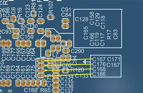
White silkscreen has long served as the standard method for applying legends, component identifiers, and traceability marks on printed circuit boards. Engineers often encounter situations where this approach falls short in durability, adhesion on certain substrates, or compatibility with high-temperature processes. Alternatives such as laser marking PCB, inkjet printing PCB, etching PCB, engraving PCB, and labeling PCB provide targeted solutions that address these limitations while maintaining compliance with industry expectations for legibility and permanence. Selection among these options depends on board material, production volume, environmental exposure, and downstream assembly requirements. Each method introduces distinct trade-offs in cost, speed, and long-term reliability that design and manufacturing teams must evaluate systematically.
Why Marking Alternatives Matter in PCB Production
Markings on PCBs enable component placement verification, quality inspection, and field traceability throughout the product lifecycle. Traditional white silkscreen ink can degrade under thermal cycling, chemical exposure, or mechanical abrasion, leading to readability issues during automated optical inspection or repair operations. In high-reliability applications, such as aerospace or automotive electronics, permanent identification becomes essential to satisfy qualification criteria outlined in IPC-6012E. Alternative marking techniques allow engineers to achieve consistent contrast and adhesion on diverse laminate finishes, including those with low surface energy or heavy copper features. These methods also support finer feature sizes required for dense layouts where space for conventional legends is limited.
Technical Principles of Laser Marking PCB
Laser marking PCB relies on a focused beam to alter the surface of the solder mask or copper layer through ablation, annealing, or color change. The process creates high-contrast characters or barcodes without adding material, which eliminates risks associated with ink delamination. Engineers select laser parameters such as wavelength, pulse duration, and power density to match the specific mask chemistry and underlying substrate. This technique produces marks that withstand reflow temperatures and cleaning chemistries commonly encountered in surface-mount assembly. Because the marking occurs after solder mask application, it integrates easily into existing fabrication sequences while preserving the integrity of fine-pitch features.
Mechanisms Behind Inkjet Printing PCB
Inkjet printing PCB deposits specialized inks directly onto the board surface using precision print heads. The inks are formulated for rapid curing under ultraviolet light or thermal exposure, forming durable legends that bond to the solder mask. This non-contact method accommodates irregular board contours and supports variable data printing, such as serial numbers generated on demand. Resolution depends on droplet size and head positioning accuracy, enabling character heights suitable for both manual and machine-readable formats. Process control focuses on ink viscosity, substrate temperature, and curing energy to prevent smearing or incomplete polymerization during subsequent handling.
Etching PCB and Engraving PCB Approaches
Etching PCB removes material from the copper or mask layer through chemical or plasma processes to create recessed or contrasting marks. The technique integrates with existing photolithographic steps, allowing legends to be defined in the same artwork as circuit patterns. Engraving PCB employs mechanical or laser-assisted tools to physically cut into the surface, producing raised or recessed characters with tactile feedback. Both methods deliver permanent identification that survives aggressive cleaning and thermal stress without relying on added coatings. Engineers must account for potential impact on electrical performance, such as changes in trace impedance or mask thickness, when specifying these techniques.
Labeling PCB as a Complementary Option
Labeling PCB applies pre-printed or on-demand adhesive labels that carry text, barcodes, or QR codes. This approach suits low-volume or prototype runs where permanent surface modification is undesirable. Labels must meet adhesion and temperature-resistance criteria to remain intact through reflow, wave soldering, and conformal coating operations. Material selection includes polyimide or polyester films with acrylic adhesives engineered for electronics environments. Engineers verify label compatibility with automated placement equipment and ensure that the final assembly process does not obscure or damage the applied identifiers.
Practical Considerations for Selecting a Marking Method
Design teams evaluate marking options against board finish, expected service conditions, and inspection requirements. High-volume production often favors laser marking PCB or inkjet printing PCB for speed and consistency, while etching PCB or engraving PCB suits applications demanding maximum permanence. Labeling PCB provides flexibility during early development stages or when frequent design revisions occur. Regardless of method, markings should remain legible after all manufacturing steps, including cleaning and coating, to support traceability mandated by quality management systems. Process validation typically includes accelerated aging tests that simulate thermal, humidity, and mechanical stresses encountered in end-use environments.
Best Practices for Implementation
Engineers document marking specifications in fabrication drawings, including font size, contrast requirements, and location tolerances. Early collaboration between design and manufacturing teams helps identify potential conflicts with component placement or test fixtures. Process monitoring during production confirms that each marking technique meets acceptance criteria for contrast, adhesion, and dimensional accuracy. When multiple methods are combined on a single board, compatibility between processes, such as laser marking after inkjet printing, requires careful sequencing to avoid interference.
Conclusion
Alternative marking techniques expand the options available when white silkscreen proves insufficient for durability or process compatibility. Laser marking PCB, inkjet printing PCB, etching PCB, engraving PCB, and labeling PCB each offer unique advantages that align with specific production and reliability needs. Systematic evaluation against board materials, environmental demands, and inspection protocols enables informed selection. Consistent application of these methods supports traceability and quality objectives throughout the PCB lifecycle.
FAQs
Q1: What advantages does laser marking PCB provide compared with traditional silkscreen?
A1: Laser marking PCB creates permanent, high-contrast identifiers directly on the solder mask or copper without added material. The process withstands reflow temperatures and cleaning chemistries while supporting fine feature sizes required on dense layouts. Engineers often select this method when long-term legibility under thermal or mechanical stress is critical.
Q2: How does inkjet printing PCB differ from etching PCB in terms of durability?
A2: Inkjet printing PCB applies a cured ink layer that bonds to the surface, offering good contrast and flexibility for variable data. Etching PCB removes material to form recessed marks that integrate with the base copper or mask, providing maximum resistance to abrasion and chemicals. Choice between the two depends on whether surface addition or material removal better suits the application environment.
Q3: When is labeling PCB preferred over engraving PCB?
A3: Labeling PCB allows quick application of identifiers without altering the board surface, making it suitable for prototypes or low-volume runs with frequent revisions. Engraving PCB produces mechanically cut marks that remain intact through aggressive processing but requires dedicated tooling and may affect nearby features. Engineers weigh setup time, permanence needs, and production volume when deciding between these approaches.
Q4: What standards guide the acceptability of markings produced by these alternative methods?
A4: Acceptability criteria for PCB markings appear in IPC-A-600K, which addresses legibility, contrast, and location requirements regardless of the application technique. Additional guidance on overall board qualification is provided in IPC-6012E. These documents help ensure that laser marking PCB, inkjet printing PCB, etching PCB, engraving PCB, or labeling PCB results meet inspection expectations.
References
IPC-6012E — Qualification and Performance Specification for Rigid Printed Boards. IPC, 2017
IPC-A-600K — Acceptability of Printed Boards. IPC, 2020


