 ALLPCB


VR headsets integrate high-resolution displays, motion sensors, wireless modules, and power management circuits into a compact, lightweight form factor. The PCB layout directly influences signal integrity, thermal performance, electromagnetic compatibility, and overall user experience. Engineers must balance electrical requirements with mechanical constraints such as limited board space and weight targets. Effective VR headset PCB layout practices ensure reliable operation during extended use while meeting strict power and latency targets.
In VR applications, data rates between the display driver and processor can exceed several gigabits per second, while inertial measurement units demand low-noise analog paths. Poor layout choices introduce crosstalk, impedance mismatches, or ground bounce that degrade image quality and tracking accuracy. Compact enclosures also limit airflow, making heat spreading through copper planes and component arrangement essential. These factors make VR headset PCB layout a specialized discipline within high-speed digital design.
Why PCB Layout Matters for VR Headsets
In VR applications, data rates between the display driver and processor can exceed several gigabits per second, while inertial measurement units demand low-noise analog paths. Poor layout choices introduce crosstalk, impedance mismatches, or ground bounce that degrade image quality and tracking accuracy. Compact enclosures also limit airflow, making heat spreading through copper planes and component arrangement essential. These factors make VR headset PCB layout a specialized discipline within high-speed digital design.
Core Engineering Principles
Signal integrity begins with controlled impedance traces and proper return paths. Differential pairs for high-speed interfaces require matched lengths and consistent reference planes to minimize skew and reflections. Analog sensor circuits benefit from separation from digital switching noise through strategic partitioning of the board. Power distribution networks must supply stable voltage to processors and displays without excessive voltage drop or ripple under dynamic loads.
Thermal considerations arise because VR headsets operate in close proximity to the user’s face. Heat-generating components such as application processors and display drivers require placement that allows heat spreading toward the edges or dedicated thermal vias. Electromagnetic interference between wireless radios and sensitive receiver circuits must be managed through shielding and frequency planning. These principles align with established design practices outlined in IPC-2221.
Component Placement Guidelines for VR Headsets
Place high-speed components such as display drivers and memory close to their respective connectors or flex interfaces to shorten critical traces. Keep analog sections, including sensor interfaces, physically distant from digital domains and switching power supplies. Position heat-sensitive components away from major heat sources and orient them to benefit from any available airflow or heat-spreading copper areas.
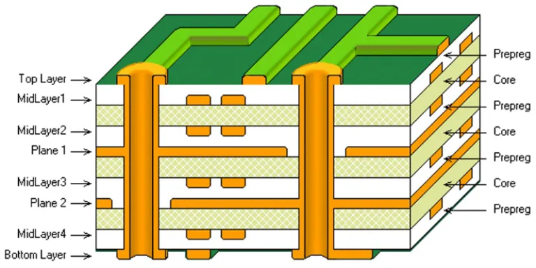
Group related functions on the same layer or adjacent layers when possible to reduce via counts. Maintain adequate clearance around antennas and RF modules to preserve radiation patterns. These placement decisions reduce the need for excessive routing layers and help achieve the thin stack-ups typical in wearable devices.
Signal Routing Best Practices
Route high-speed differential pairs on inner layers adjacent to solid reference planes whenever possible. Maintain consistent trace width and spacing to achieve target impedance, typically 85 or 100 ohms for many VR display interfaces. Avoid sharp bends and unnecessary vias that can cause impedance discontinuities.
For clock and data lines, match lengths within tight tolerances to preserve timing margins. Separate sensitive analog traces from digital aggressors by at least three times the trace width or use guard traces where space permits. Ground stitching vias placed near signal transitions help maintain continuous return paths.
Ground Plane and Power Distribution Strategies
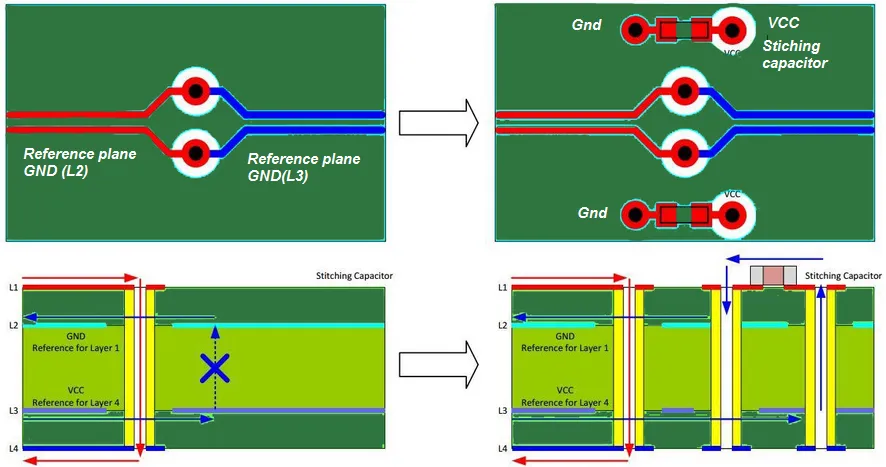
A continuous, low-impedance ground plane serves as the foundation for both signal return paths and EMI control in VR headset PCB layout. Divide the ground plane only when necessary to isolate noisy digital sections from sensitive analog areas, then reconnect with narrow bridges or stitching capacitors. Multiple ground planes in a multilayer stack-up further reduce inductance for high-frequency returns.
Power planes or wide traces should be sized according to current requirements and placed adjacent to ground planes to form low-inductance capacitor structures. Decoupling capacitors must be located as close as possible to power pins, with vias connecting directly to the planes. These practices support stable operation under the varying loads typical of VR content rendering.
Thermal and EMI Considerations
Thermal vias under hot components conduct heat to inner copper layers or external heatsinks. Copper pours connected to ground or dedicated thermal nets increase the effective heat-spreading area without adding significant weight. Component orientation and board edge placement can direct heat away from the user’s face.
EMI mitigation includes proper shielding can placement, filtered power entry points, and careful routing of cables that exit the enclosure. Following qualification requirements such as those in IPC-6012 helps verify that the finished board maintains performance after environmental stresses.
Conclusion
Successful VR headset PCB layout integrates signal integrity, thermal management, and EMI control within severe space and weight constraints. Logical component placement, disciplined routing, and robust ground plane design form the basis for reliable high-performance operation. Adherence to recognized industry standards supports consistent manufacturing outcomes and long-term product reliability.
FAQs
Q1: What factors define effective VR headset PCB layout?
A1: Effective VR headset PCB layout addresses high-speed signal integrity, thermal dissipation, and electromagnetic compatibility within a compact form factor. Engineers focus on controlled impedance routing, strategic component placement, and continuous ground planes to maintain display quality and sensor accuracy while managing power and heat.
Q2: How does component placement influence VR headset performance?
A2: Component placement determines trace lengths, thermal paths, and noise coupling. Positioning high-speed devices near connectors reduces signal degradation, while separating analog sensors from digital circuits improves tracking precision and overall system stability.
Q3: Why is the ground plane critical in VR PCB design?
A3: A solid ground plane provides low-impedance return paths for high-speed signals and helps contain electromagnetic emissions. Proper ground plane design reduces crosstalk and supports stable power delivery to processors and displays under dynamic operating conditions.
Q4: What routing practices support signal integrity in VR headsets?
A4: Routing practices include matched-length differential pairs, consistent reference planes, and minimized via counts on critical nets. These techniques preserve timing margins and reduce reflections that could otherwise affect image quality or wireless performance.
References
IPC-2221 — Generic Standard on Printed Board Design. IPC.
IPC-6012E — Qualification and Performance Specification for Rigid Printed Boards. IPC, 2017.


