 ALLPCB


Understanding Solder Mask Expansion for Matte Finishes
Solder mask expansion plays a critical role in printed circuit board design, particularly when matte finishes are specified. Matte solder masks provide reduced reflectivity and improved visual contrast during automated optical inspection, yet they require careful management of expansion parameters to maintain electrical integrity and manufacturability. Engineers must balance the need for adequate clearance around copper features with the constraints imposed by registration tolerances and material behavior during curing. Proper handling of these factors helps prevent issues such as exposed copper or mask encroachment on pads. The topic intersects directly with established PCB design practices that prioritize both performance and yield.
What Is Solder Mask Expansion and Why It Matters
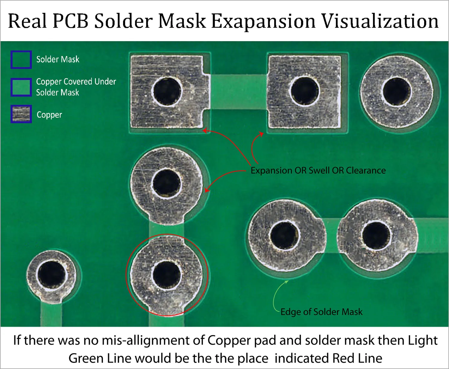
Solder mask expansion refers to the intentional enlargement of the mask opening relative to the underlying copper pad or trace. This enlargement compensates for alignment variations that occur between the imaging step and the final copper pattern. In matte finishes the expansion value often follows specific design rules that differ from glossy counterparts because of differences in coating thickness and surface texture. Adequate expansion ensures that the mask does not cover any portion of the pad intended for soldering, thereby supporting reliable component attachment. Insufficient expansion can lead to reduced solderable area, while excessive expansion increases the risk of solder bridging between adjacent features. Industry standards such as IPC-6012E address qualification requirements that include mask registration and clearance considerations.

Technical Principles of Solder Mask Expansion
The mechanism of solder mask expansion begins with the photolithographic process used to define mask openings. A negative or positive image is aligned to the copper pattern, and any offset between the two layers must be absorbed by the expansion allowance. Matte masks are typically applied at slightly greater thicknesses than glossy versions to achieve the desired low-gloss appearance, which can influence the minimum reliable expansion distance. Thermal expansion of the mask material during curing and subsequent reflow cycles further affects final dimensions. Designers therefore calculate expansion based on the cumulative tolerances of imaging equipment, board material shrinkage, and mask application method. These calculations directly influence PCB clearances and must remain consistent with the pad size calculation used for each component footprint.
Design Rules and Pad Size Calculation for Matte Solder Masks
Matte solder mask design rules commonly specify minimum expansion values that account for both registration accuracy and the physical properties of the cured mask. A typical approach starts with the nominal pad diameter and adds an expansion value on each side to determine the mask opening size. This value is then verified against the minimum annular ring requirements and the spacing needed to avoid mask-defined versus copper-defined pads. When performing pad size calculation, engineers incorporate the chosen expansion to ensure that the final soldermask opening remains large enough for acceptable solder fillet formation. Adjustments may be necessary for fine-pitch components where the available space between pads limits the maximum expansion that can be applied without compromising solder bridging prevention. Consistent application of these rules across a design improves overall manufacturability.
Preventing Solder Bridging Through Proper Clearances
Solder bridging occurs when molten solder unintentionally connects two or more conductors during assembly. Proper solder mask expansion contributes to solder bridging prevention by maintaining a minimum distance between the mask-defined openings of adjacent pads. The mask acts as a barrier that contains the solder within each opening, provided the expansion has been sized correctly relative to the pad-to-pad spacing. In matte finishes the surface texture can influence solder flow characteristics, making adherence to recommended clearances especially important. Designers evaluate the worst-case registration tolerance when setting expansion values so that even under maximum misalignment the mask still provides adequate separation. This structured evaluation reduces the likelihood of shorts and supports higher assembly yields.
Best Practices for Matte Solder Mask Implementation
Effective implementation begins with early collaboration between the design and fabrication teams to confirm the exact expansion values supported by the chosen matte mask process. Documentation should clearly specify both the expansion value and the measurement method, typically from the edge of the copper feature to the edge of the mask opening. Review of the complete set of PCB clearances ensures that no trace or via falls within the expanded mask region unless intended. Simulation of thermal profiles during reflow can further validate that the chosen expansion remains stable under operating conditions. Regular verification against IPC-A-600K acceptability criteria helps confirm that finished boards meet visual and dimensional requirements for matte mask applications.
Conclusion
Solder mask expansion for matte finishes requires deliberate attention to registration tolerances, material characteristics, and assembly requirements. By applying logical, standards-aligned calculations engineers can achieve reliable pad size definition while minimizing the risk of solder bridging. Consistent use of matte solder mask design rules supports both visual inspection performance and long-term board reliability. The principles outlined provide a foundation for repeatable results across a wide range of PCB designs.
FAQs
Q1: What is solder mask expansion and how does it affect matte finishes?
A1: Solder mask expansion is the controlled enlargement of mask openings beyond the copper pad edges. In matte finishes this parameter must accommodate slightly thicker coatings while still preventing mask encroachment on pads. Proper expansion values maintain PCB clearances and support consistent soldering outcomes.
Q2: How do matte solder mask design rules influence pad size calculation?
A2: Matte solder mask design rules incorporate material-specific expansion allowances into the pad size calculation process. These rules ensure that the final mask opening provides sufficient area for solder while respecting minimum spacing requirements. Following the rules consistently reduces variability in finished boards.
Q3: Why is solder bridging prevention important when using matte solder masks?
A3: Solder bridging prevention relies on adequate separation between mask openings. Matte finishes can alter surface energy and solder flow, making precise expansion values essential. Correct clearances derived from expansion calculations help contain solder within individual pad areas during reflow.
Q4: What standards guide solder mask expansion practices?
A4: Standards such as IPC-6012E and IPC-A-600K provide qualification and acceptability criteria that include mask registration and clearance expectations. These documents establish baseline requirements for expansion values and visual inspection of matte mask surfaces.





