 ALLPCB


What Are MID PCBs and Why Manufacturing Method Matters
MID technology integrates conductive traces directly onto three-dimensional plastic substrates. This approach reduces part count and assembly steps compared with traditional rigid or flexible printed circuit boards. Two-shot molding and LDS represent the primary commercial routes for creating these integrated devices. Selection influences achievable feature sizes, thermal performance, and long-term reliability in applications ranging from automotive sensors to medical devices. Factory teams evaluate both methods against volume forecasts and design constraints early in the project.
Technical Principles of Two-Shot Molding for MID PCBs
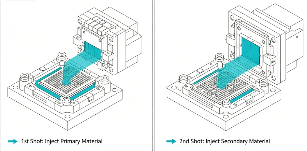
In two-shot molding, a first injection forms the structural plastic body, typically using a non-plateable resin. A second shot introduces a plateable material, often containing catalytic additives, into selected areas that will carry circuitry. After molding, electroless copper plating deposits conductive traces on the activated surfaces. The process supports complex 3D routing and undercuts that are difficult to achieve with flat substrates. Tooling must accommodate precise alignment between shots to maintain trace registration. Production runs benefit from high repeatability once molds are qualified.
Related Reading: Tackling Challenging Geometries: Solder Paste Dispensing on 3D MIDs
Technical Principles of LDS for MID PCBs
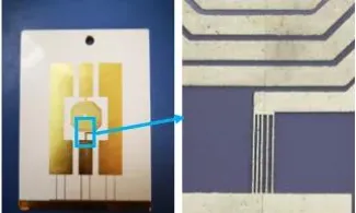
Laser direct structuring begins with a single molded part compounded with laser-activatable additives. A laser beam patterns the desired circuit layout by selectively activating the additive on the surface. Subsequent electroless plating deposits copper only on the laser-exposed areas. This method allows fine-line features and rapid design iterations without new tooling. Circuit density can reach levels suitable for high-frequency signals when material and plating parameters are controlled. LDS also accommodates modifications late in development by simply reprogramming the laser path.
Related Reading: The Benefits of Laser Direct Structuring (LDS) in Rigid Flex PCB Assembly
LDS MID PCB Comparison and Key Differences
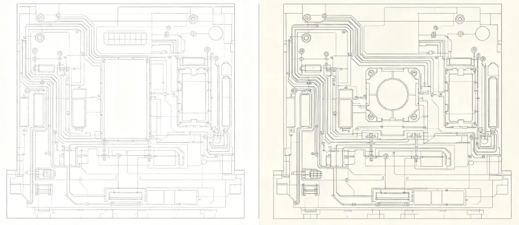
Two-shot molding excels in high-volume scenarios where the same geometry repeats thousands of times. Initial tooling investment is substantial, yet per-unit costs decline sharply after amortization. LDS offers greater flexibility for prototypes and low-to-medium volumes because circuit changes require only software updates. Feature resolution tends to favor LDS for dense layouts, while two-shot molding can produce thicker traces suited to higher current loads. Material choices also differ: two-shot processes often use paired resins with matched coefficients of thermal expansion, whereas LDS works with a broader range of single-shot engineering plastics. Both methods must address warpage control during plating and reflow to meet mechanical tolerances.
Design Considerations for MID PCBs
Engineers begin by mapping electrical and mechanical requirements onto the three-dimensional envelope. Trace width, spacing, and via placement must respect the selected process limits to avoid plating defects. Thermal expansion mismatch between resin and metal layers requires evaluation against expected operating temperatures. Surface finish options, such as immersion silver or electroless nickel gold, influence solderability and long-term corrosion resistance. Designers also consider mold flow for two-shot parts and laser accessibility angles for LDS parts. Early collaboration between electrical and mechanical teams reduces the need for costly revisions.
Cost Analysis of MID Manufacturing Methods
Tooling for two-shot molding includes precision multi-cavity molds and alignment features that increase upfront expense. Amortization over large production quantities often yields the lowest unit cost. LDS avoids dedicated circuit tooling and instead relies on laser programming time, making it economical for smaller batches or frequent design changes. Material costs vary with resin selection and plating chemistry consumption. Yield rates depend on process control; both methods require consistent surface preparation to minimize scrap. Procurement teams typically model total cost of ownership, including qualification testing and field reliability, rather than comparing only piece prices.
Best Practices in MID PCB Production
Process qualification begins with material characterization and plating bath monitoring. Statistical process control tracks critical dimensions and electrical continuity across production lots. Post-plating inspection verifies trace adhesion and insulation resistance. When volumes justify the investment, two-shot molding teams optimize cycle times through balanced runner systems and automated part handling. LDS operations focus on laser parameter stability and consistent additive dispersion within the resin. Both approaches benefit from documented work instructions aligned with factory quality systems.
Conclusion
Two-shot molding and LDS each provide reliable routes to functional MID PCBs when matched to project parameters. High-volume, stable designs favor two-shot molding for cost efficiency, while complex or evolving layouts benefit from the agility of LDS. Thorough evaluation of geometry, electrical demands, and production scale guides the final selection. Adherence to recognized industry specifications supports consistent quality across either method.
FAQs
Q1: What factors determine whether two-shot molding MID PCBs or LDS MID PCB is more suitable for a given application?
A1: Volume expectations, circuit density, and design stability are primary considerations. High-volume programs with fixed geometries typically achieve lower unit costs with two-shot molding. Projects requiring frequent revisions or fine features often proceed faster with LDS. Engineers review these elements alongside material compatibility and thermal requirements before finalizing the process.
Q2: How does the cost analysis of MID PCB manufacturing differ between two-shot molding and LDS?
A2: Two-shot molding carries higher initial tooling costs that amortize over large quantities. LDS reduces tooling expense but may increase per-unit processing time for very high volumes. Material and plating costs depend on the specific resins and chemistry selected for each method. Total cost modeling includes qualification and yield considerations for accurate comparison.
Q3: What design considerations MID PCB teams should address when comparing the two manufacturing methods?
A3: Trace geometry, three-dimensional routing freedom, and thermal expansion behavior require evaluation against process capabilities. Two-shot molding supports robust mechanical features but demands precise mold alignment. LDS provides rapid patterning flexibility yet requires attention to laser access and additive distribution. Early assessment prevents downstream manufacturing issues.
Q4: Which industry standards guide quality expectations for both two-shot molding MID PCBs and LDS MID PCB production?
A4: IPC-6012E establishes qualification and performance criteria applicable to the resulting interconnect structures. ISO 9001:2015 outlines quality management practices that support consistent process control in either manufacturing route. Compliance documentation helps ensure traceability and repeatability across production batches.
References
IPC-6012E — Qualification and Performance Specification for Rigid Printed Boards. IPC, 2017
ISO 9001:2015 — Quality Management Systems. ISO, 2015
IPC-A-600K — Acceptability of Printed Boards. IPC, 2020





