 ALLPCB


Printed circuit boards must maintain structural integrity throughout manufacturing, assembly, and end use. PCB thickness and size directly influence mechanical strength, resistance to warpage, and overall durability. Engineers balance these parameters during substrate selection to meet performance requirements without excessive material use or added weight. Larger boards experience greater bending moments under thermal or mechanical loads, making thickness a critical factor in preventing deformation. Proper coordination of these dimensions supports reliable operation in demanding environments.
Why PCB Thickness and Size Matter for Durability
PCB durability depends on the board's ability to resist bending, twisting, and thermal expansion mismatches. As board size increases, the unsupported span grows, raising the risk of deflection under its own weight or external forces. Thickness contributes to flexural rigidity because stiffness scales with the cube of thickness in beam theory. Substrate selection further modulates this behavior through material modulus and coefficient of thermal expansion. When these factors align correctly, the finished assembly maintains planarity and electrical performance over its service life.
Industry specifications such as IPC-6012E establish minimum performance criteria for rigid printed boards, including requirements related to dimensional stability and flatness. Designers reference these criteria early to avoid costly redesigns later in the process.
Technical Principles of Thickness, Size, and Mechanical Strength
Flexural rigidity of a rectangular plate increases rapidly with thickness. A board that is 1.6 mm thick exhibits roughly eight times the stiffness of a 0.8 mm board of identical material and width. This relationship becomes especially important for maximum board sizes exceeding 300 mm in any dimension, where self-weight and handling stresses can induce noticeable curvature. Thermal gradients during reflow soldering create additional stresses because copper and dielectric layers expand at different rates. Thicker constructions distribute these stresses over a greater cross-section, reducing peak strain and limiting permanent deformation.
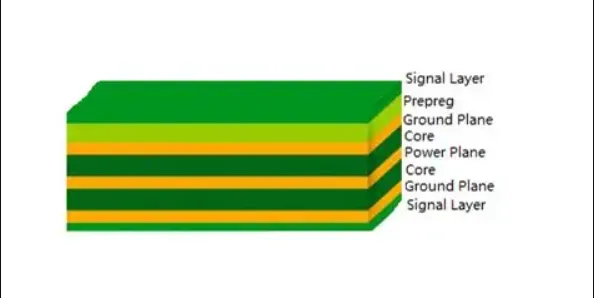
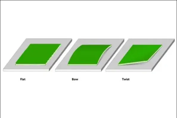
Warpage arises primarily from asymmetric copper distribution or mismatched material properties across the stack-up. Larger panels amplify any imbalance because the moment arm from the neutral axis to the outer fibers grows with size. IPC-A-600K provides visual and quantitative acceptance criteria for bow and twist, helping manufacturers verify that finished boards remain within allowable limits. Substrate selection plays a decisive role here; higher-modulus cores or balanced copper weights on both sides improve resistance to thermally induced warpage.

Mechanical strength also encompasses resistance to vibration and shock. Thicker boards lower the natural frequency of vibration modes, moving resonant frequencies away from common operating environments. This effect is pronounced in larger boards that would otherwise behave like flexible diaphragms. Proper thickness therefore contributes to both static and dynamic durability without requiring additional stiffeners or mounting hardware.
Best Practices for Balancing Thickness and Maximum Size
Begin with a clear definition of maximum board dimensions and expected environmental loads. Calculate approximate deflection using plate theory or finite-element analysis to determine the minimum thickness that keeps bow and twist within IPC-A-600K limits. Increase thickness in 0.2 mm or 0.4 mm increments rather than jumping to the next standard value, because each step yields substantial stiffness gains.
Select substrate materials with appropriate glass-transition temperature and modulus for the anticipated thermal profile. Balanced copper distribution on outer layers and symmetric inner-layer construction minimize built-in stresses. When maximum size approaches the limits of standard panel formats, consider adding non-functional copper or stiffening ribs on non-critical areas to enhance rigidity without changing overall thickness.
During layout, maintain adequate clearance from board edges for mounting holes and connectors. These features act as stress concentrators; thicker material around them improves load distribution. Review stack-up symmetry early with the fabricator to confirm that the chosen thickness supports the required number of layers while preserving flatness after lamination and reflow.
Process controls during fabrication further protect durability. Controlled cooling rates after lamination and reflow reduce residual stresses. Panel designs that incorporate breakaway tabs or support rails help maintain flatness until individual boards are separated. These measures complement the inherent stiffness provided by adequate thickness.
Conclusion
PCB thickness and maximum size interact through fundamental mechanical relationships that govern stiffness, thermal stability, and resistance to warpage. Thoughtful substrate selection combined with adherence to recognized industry specifications enables engineers to achieve durable designs without unnecessary material overhead. Early analysis of deflection limits and stack-up symmetry prevents downstream quality issues. The result is a board that maintains planarity and electrical integrity throughout its intended life cycle.
FAQs
Q1: How does PCB thickness influence board warpage prevention during assembly?
A1: Thicker constructions increase flexural rigidity, reducing the deflection caused by thermal gradients and copper imbalance. This effect becomes more pronounced as maximum board size increases, because larger unsupported spans amplify any tendency to bow. Balanced substrate selection and symmetric stack-ups further enhance warpage resistance when thickness is chosen appropriately.
Q2: What role does substrate selection play in mechanical strength of PCBs?
A2: Substrate choice determines modulus, thermal expansion characteristics, and glass-transition behavior, all of which interact with thickness to set overall rigidity. Higher-modulus materials paired with adequate thickness provide greater resistance to bending and vibration, especially on larger boards. Proper selection ensures the finished assembly meets durability expectations without excessive weight.
Q3: Why must designers consider both PCB thickness and size together?
A3: Stiffness scales with the cube of thickness, yet the moment arm grows linearly with size. A thin board that performs adequately at small dimensions may exhibit unacceptable warpage or deflection when scaled to maximum size. Coordinated selection of thickness and substrate prevents these issues while satisfying mechanical and thermal requirements.
Q4: How do industry standards guide acceptable limits for PCB durability?
A4: Specifications such as IPC-6012E define performance thresholds for dimensional stability and flatness that apply across varying thicknesses and sizes. Acceptance criteria in IPC-A-600K translate these requirements into measurable bow and twist limits. Designers use these references to establish thickness targets that keep finished boards within allowable tolerances.
References
IPC-6012E — Qualification and Performance Specification for Rigid Printed Boards
IPC-A-600K — Acceptability of Printed Boards





