 ALLPCB


Introduction
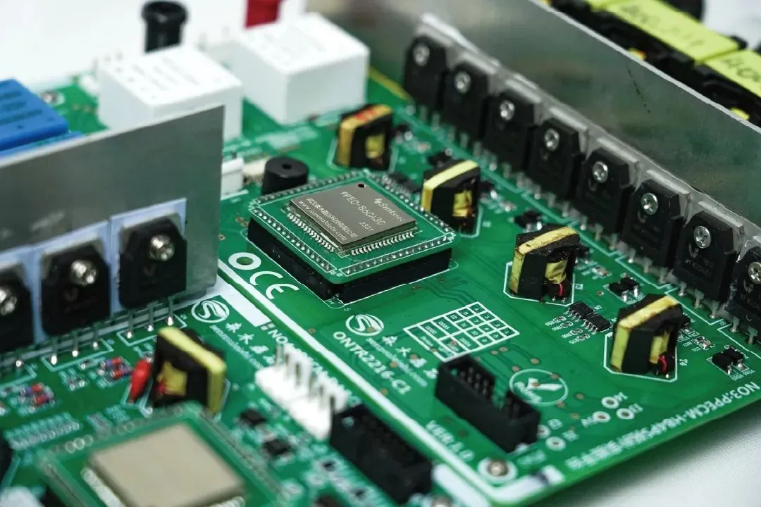
High-power power supply printed circuit boards operate under demanding conditions with substantial current flows and switching frequencies that generate significant heat. Effective power supply PCB thermal design prevents overheating, which can degrade components like MOSFETs, inductors, and diodes, leading to reduced efficiency and premature failures. Engineers must prioritize power supply PCB heat dissipation to ensure long-term reliability in applications such as industrial inverters, electric vehicle chargers, and server power units. Key elements include strategic component placement, enhanced copper structures, and auxiliary cooling methods. This article explores proven strategies tailored for electric engineers, focusing on thermal vias and heat sinks while adhering to established industry practices. By implementing these approaches, designers can optimize thermal performance without compromising electrical integrity.
Why Thermal Management Matters in Power Supply PCBs
Power supply PCBs in high-power systems face unique thermal challenges due to concentrated heat sources from power semiconductors and magnetic components. Elevated temperatures accelerate electromigration in traces, increase leakage currents in semiconductors, and compromise solder joint integrity over time. Inadequate power supply PCB thermal design results in derating components below their rated capacities, shortening operational lifespan and raising maintenance costs. Compliance with standards like IPC-2221 ensures designs meet minimum thermal relief requirements for safe operation. Moreover, effective heat management supports higher power densities, enabling compact enclosures critical for modern electronics. Engineers must balance thermal constraints with electrical performance to avoid hotspots that propagate failures across the board.
Thermal runaway poses a severe risk in power supplies, where localized overheating can cascade into system-wide shutdowns or safety hazards. Simulations and prototypes reveal that unaddressed heat buildup exceeds junction temperatures specified by component datasheets, violating reliability benchmarks. Power supply PCB heat dissipation strategies directly influence mean time between failures, a key metric for mission-critical deployments. Prioritizing thermal vias and heat sinks early in the design phase mitigates these issues, fostering robust products.
Fundamental Principles of Heat Transfer in Power Supply PCBs
Heat in power supply PCBs primarily arises from I-squared-R losses in conductors, switching inefficiencies in transistors, and core losses in transformers. Conduction dominates within the board, governed by Fourier's law where heat flux is proportional to the temperature gradient and material conductivity. Copper layers and planes serve as primary heat spreaders due to their high thermal conductivity, distributing heat evenly to prevent localized hotspots. Thermal resistance, quantified as theta (junction-to-ambient), guides design decisions for overall dissipation paths. Radiation and convection play secondary roles, enhanced by board geometry and airflow.
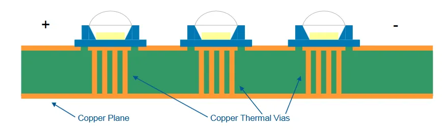
In multilayer boards, vertical heat transfer relies on vias to bridge layers, effectively coupling inner planes for dissipation. Horizontal spreading occurs through wide traces and pours, sized according to empirical data from standards like IPC-2152 for acceptable temperature rises. Natural convection depends on surface area and orientation, while forced air amplifies cooling in enclosed systems. Understanding these mechanisms allows engineers to model thermal profiles accurately during layout. Power supply PCB thermal vias exploit conduction to inner copper planes, reducing effective thermal resistance significantly.
Key Strategies for Power Supply PCB Thermal Design
Optimizing copper utilization forms the foundation of power supply PCB thermal design. Thick copper layers, such as 2 oz or heavier, increase cross-sectional area for both current handling and heat spreading. Solid ground or power planes on multiple layers provide low-impedance thermal paths, stitching adjacent planes with via arrays to minimize resistance. Engineers should allocate dedicated plane layers beneath high-power components to capture and redistribute heat. This approach aligns with guidelines in IPC-2221 for enhancing board-level thermal performance. Careful routing avoids narrow necks that bottleneck heat flow.
Thermal vias represent a critical enabler for power supply PCB heat dissipation, particularly under packages with exposed pads like QFNs and power SOICs. Arrays of 10 to 20 vias, placed directly beneath the heat source, transfer heat to opposing or inner layers efficiently. Via dimensions typically feature small diameters for density, with plating thickness ensuring mechanical robustness during reflow. Filling vias with conductive epoxy further reduces thermal resistance, ideal for high-reliability applications. Placement patterns should fan out from the pad to avoid solder wicking issues. Testing confirms these structures lower component temperatures by coupling to chassis grounds.
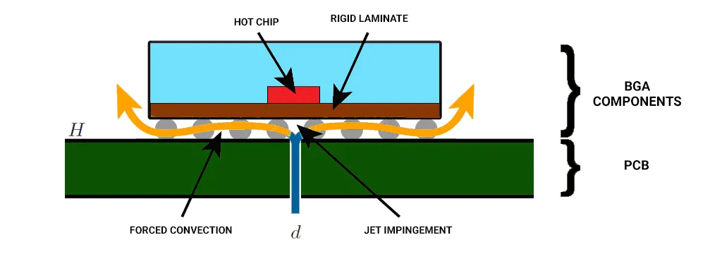
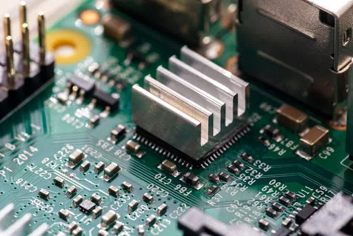
Heat sinks integrate seamlessly with power supply PCB thermal vias to boost convection cooling. Aluminum or copper extrusions attach via clips, screws, or adhesives to components or board areas, fins oriented parallel to airflow. Thermal interface materials, such as gap pads or pastes, minimize air gaps at the interface, crucial for low thermal resistance. For board-level sinks, vias feed heat to the underside where the sink mounts, creating a composite dissipation path. Engineers must calculate sink size based on required theta, factoring ambient conditions and airflow velocity. Hybrid solutions combine sinks with fans for extreme power levels.
Component layout profoundly impacts overall thermal gradients. Positioning heat sources near board edges facilitates edge cooling, while spacing them apart prevents mutual heating. Sensitive low-power ICs reside away from hotspots, routed on cooler layers. Airflow simulation guides ducting and fenestration in enclosures. Multi-layer stackups dedicate inner layers for isolation and heat sinking.
Advanced Best Practices and Implementation Considerations
Beyond basics, embedded heat pipes or metal slugs offer superior conduction in ultra-high-power designs, though they demand precise fabrication tolerances. Via tenting preserves solder paste volume while allowing heat escape, a technique refined through iterative prototyping. Finite element analysis verifies designs pre-fabrication, predicting hotspots under load. Qualification per IPC-6012 ensures boards withstand thermal cycling without delamination.
Troubleshooting hotspots involves infrared thermography during powered testing, identifying via inefficiencies or plane voids. Iterative refinements, such as adding capacitance for ripple reduction, indirectly aid cooling by stabilizing currents. Documentation of thermal models supports design reuse across power variants.
Conclusion
Mastering thermal management in high-power power supply PCBs demands a holistic approach integrating copper optimization, power supply PCB thermal vias, and heat sinks. These strategies ensure reliable operation by controlling temperatures within safe limits, extending system life. Adhering to IPC guidelines provides a structured path to compliant designs. Engineers benefit from early thermal awareness in layout, validated through analysis and testing. Ultimately, robust power supply PCB heat dissipation unlocks higher performance densities for demanding applications.
FAQs
Q1: What role do thermal vias play in power supply PCB thermal design?
A1: Thermal vias facilitate vertical heat transfer from top-side components to inner copper planes or the board underside in power supply PCB thermal design. Arrays under hot pads reduce junction temperatures by distributing heat across layers. Optimal configurations use small diameters with sufficient density to balance thermal and electrical performance. Filling enhances reliability in vibration-prone environments. This method complies with design principles for multilayer heat management.
Q2: How can heat sinks improve power supply PCB heat dissipation?
A2: Heat sinks enhance power supply PCB heat dissipation through increased surface area for convection, attached via thermal interfaces to components or via-linked board areas. Proper fin orientation aligns with airflow for maximum effectiveness. Combined with power supply PCB thermal vias, they form low-resistance paths to ambient. Selection considers power dissipation and enclosure constraints. Mechanical securement prevents detachment under thermal expansion.
Q3: What factors influence power supply PCB thermal vias effectiveness?
A3: Effectiveness of power supply PCB thermal vias depends on array density, plating quality, and connection to spreading planes. Placement directly under heat sources minimizes path length. Multiple layers amplify coupling capacity. Avoiding solder fill in non-critical areas preserves cost. Integration with overall layout prevents airflow blockage.
Q4: Why is copper plane usage essential in power supply PCB thermal design?
A4: Copper planes in power supply PCB thermal design spread heat horizontally with high conductivity, sized per current-carrying guidelines. They couple via fields for vertical relief. Stitching vias interconnect layers seamlessly. This foundation supports heat sinks and natural cooling efficiently.
References
IPC-2221B - Generic Standard on Printed Board Design. IPC, 2012
IPC-2152A - Standard for Determining Current Carrying Capacity in Printed Board Design. IPC, 2009
IPC-6012E - Qualification and Performance Specification for Rigid Printed Boards. IPC, 2015


