 ALLPCB


Introduction
In modern PCB design, achieving precise control over signal integrity demands meticulous attention to stackup parameters. Core thickness plays a pivotal role in determining characteristic impedance, mechanical stability, and overall board performance. Engineers rely on PCB calculators to perform core thickness calculations, ensuring traces meet target impedance values without trial-and-error iterations. These online PCB calculators and PCB design tools simplify complex computations involving PCB trace width, dielectric constant, and layer configurations. As high-speed signals push frequencies higher, mismatches in core thickness can lead to reflections, crosstalk, and failures. This article explores the principles behind core thickness calculation and PCB impedance calculation, providing structured guidance for electric engineers.
What Is PCB Core Thickness and Why It Matters
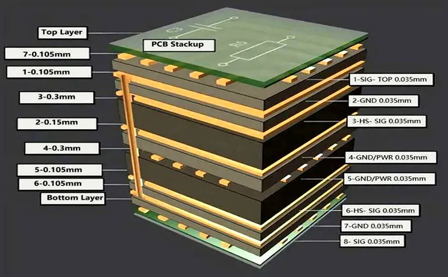
PCB core thickness refers to the dimension of the rigid, fully cured laminate sections that form the foundation of multilayer boards. These cores separate signal layers and provide structural integrity, distinguishing them from prepregs, which are semi-cured sheets used to bond layers during lamination. Selecting the appropriate core thickness directly influences PCB impedance calculation, as it defines the dielectric height between traces and reference planes. In high-speed designs, improper core thickness leads to impedance discontinuities, signal degradation, and compliance issues with industry requirements.
Beyond electrical performance, core thickness affects mechanical properties like warpage and rigidity. Thinner cores reduce overall board thickness for compact applications but increase susceptibility to thermal stresses during soldering. Thicker cores enhance stability and heat dissipation yet complicate impedance matching for fine-pitch traces. Balancing these factors ensures reliable operation in demanding environments, making core thickness calculation essential for every stackup design.
Technical Principles of Core Thickness in Impedance Control
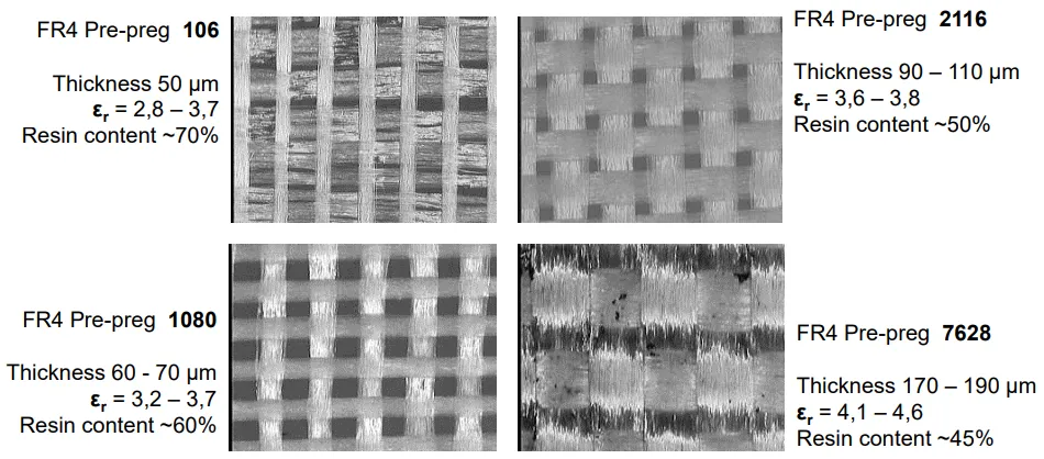
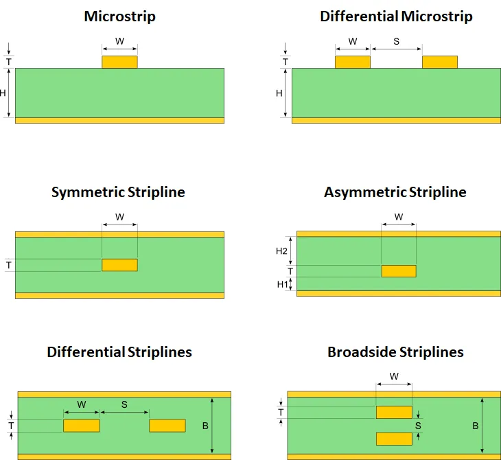
Characteristic impedance in PCBs arises from the interaction between trace geometry and the surrounding dielectric. For microstrip configurations, where traces run on outer layers over a dielectric, the impedance depends on PCB trace width, copper thickness, dielectric constant, and the height to the reference plane, often dictated by core thickness. Stripline structures, embedded between two ground planes, rely even more heavily on core thickness as the symmetric or asymmetric spacing determines the field distribution. The dielectric constant, typically influenced by resin content and glass weave, modulates the effective permittivity, further tying core selection to precise PCB impedance calculation.
Industry guidelines like IPC-2141 outline equations for these configurations, accounting for variables such as trace width over height ratios and manufacturing tolerances. For instance, increasing core thickness lowers impedance for a fixed trace width by expanding the electromagnetic field. Conversely, higher dielectric constants reduce impedance, necessitating adjustments in core thickness to compensate. Copper roughness and plating also introduce minor variations, emphasizing the need for PCB design tools that incorporate these factors.
Core thickness impacts not just impedance but also crosstalk and return loss. In dense multilayer boards, uniform core thicknesses maintain consistent dielectric heights across layers, minimizing skew in differential pairs. Thermal expansion coefficients between core materials and copper must align to prevent delamination under reflow cycles. These principles underscore why electric engineers prioritize accurate core thickness calculation early in the design phase.
Practical Solutions: Leveraging PCB Calculators for Core Thickness
Engineers begin core thickness calculation by defining target impedance, often 50 ohms single-ended or 100 ohms differential for high-speed interfaces. Input parameters into a PCB calculator include desired PCB trace width based on current carrying needs, copper weight, dielectric constant from material datasheets, and total board thickness constraints. The tool iterates stackup options, suggesting core and prepreg combinations that achieve the impedance within tolerances like plus or minus 10 percent. Online PCB calculators excel here, providing instant feedback without full PCB design software setup.
Validation follows computation through time-domain reflectometry simulations or field solvers integrated into PCB design tools. Adjust for fabrication realities, such as core thickness availability in standard increments like 0.1 mm steps. Symmetric stackups, with mirrored cores above and below the neutral axis, mitigate warpage per IPC-2221 guidelines. Document the stackup fully, specifying dielectric constants and thicknesses to guide manufacturers.
Best practices include starting with coarser grids for initial layers and finer cores for inner high-speed signals. Account for solder mask effects on outer microstrips, which slightly lower effective dielectric constant. Cross-check calculations against multiple tools to confirm consistency. This methodical approach ensures manufacturability and performance.
- Core Thickness — Typical Range: 0.1–1.6 mm — Impact on Impedance: Increases spacing, lowers Z0
- Dielectric Constant (Er) — Typical Range: 3.5–4.5 — Impact on Impedance: Higher Er lowers Z0
- Trace Width — Typical Range: 0.1–0.5 mm — Impact on Impedance: Wider trace lowers Z0
- Copper Thickness — Typical Range: 18–70 μm — Impact on Impedance: Thicker copper slightly lowers Z0
Case Study: Optimizing Core Thickness for a High-Speed Multilayer Board
Consider a 6-layer PCB for a data interface requiring 100-ohm differential impedance on inner layers. Initial PCB impedance calculation reveals that a 0.2 mm core yields excessive impedance due to tight spacing. Switching to a 0.3 mm core, paired with adjusted PCB trace widths and verified dielectric constant, aligns values within specifications. Simulations confirm minimal crosstalk, with symmetric placement preventing warpage.
Fabrication feedback highlights the importance of IPC-2141-compliant test coupons for verification. Post-lamination, measured impedances match predictions, validating the core thickness calculation. This scenario demonstrates how PCB design tools streamline iterations, reducing design cycles from weeks to days.
Conclusion
Mastering core thickness calculation elevates PCB design from guesswork to precision engineering. By integrating PCB calculators with principles from standards like IPC-2141 and IPC-2221, engineers achieve controlled impedance, mechanical reliability, and signal integrity. Focus on key variables—PCB trace width, dielectric constant, and stackup symmetry—while leveraging online PCB calculators for efficiency. These practices ensure boards perform reliably in high-speed applications. Prioritize early stackup planning to avoid costly respins and unlock optimal designs.
FAQs
Q1: What is a PCB core thickness calculator and how does it support PCB impedance calculation?
A1: A PCB core thickness calculator is a tool within PCB design software or online platforms that computes dielectric heights needed for target impedances. It uses inputs like PCB trace width, dielectric constant, and copper thickness to suggest core and prepreg combinations. This streamlines stackup design, ensuring compliance with high-speed requirements while considering manufacturing tolerances. Engineers save time by iterating virtually before fabrication.
Q2: How does dielectric constant influence core thickness calculation in multilayer PCBs?
A2: Dielectric constant affects the speed of signal propagation and impedance, requiring thicker cores to compensate for higher Er values and maintain target Z0. In core thickness calculation, tools adjust heights based on material properties to balance field confinement. This prevents mismatches in mixed-signal boards. Always verify with fab data for resin variations.
Q3: Why is PCB trace width critical in conjunction with core thickness for impedance control?
A3: PCB trace width determines current capacity and interacts with core thickness to set characteristic impedance. Narrower traces demand thinner cores for higher Z0, while wider ones allow thicker cores. Calculations per industry guidelines optimize both for signal integrity and routing density. Balance with thermal and mechanical constraints.
Q4: What role do PCB design tools play in online PCB calculator workflows?
A4: PCB design tools integrate online PCB calculators for real-time stackup optimization and impedance verification. They simulate fields, export fab drawings, and flag warpage risks from asymmetric cores. This end-to-end approach enhances precision for electric engineers handling complex multilayer designs.
References
IPC-2141A — Controlled Impedance Circuit Boards and High Speed Logic Design. IPC.
IPC-2221B — Generic Standard on Printed Board Design. IPC.
IPC-6012E — Qualification and Performance Specification for Rigid Printed Boards. IPC, 2017.


