 ALLPCB


Introduction
Controlled depth drilling, often referred to as back drilling, plays a critical role in modern PCB manufacturing, especially for high-speed applications. This technique removes unused portions of plated through-holes, known as stubs, to enhance signal performance. However, controlled depth drilling problems frequently arise, leading to PCB drilling defects that compromise reliability. Engineers encounter issues like misalignment, incomplete stub removal, and hole wall irregularities, which can trigger signal integrity issues. Addressing these PCB manufacturing errors requires a deep understanding of process variables and inspection methods. Factory-driven insights reveal that proactive troubleshooting minimizes rework and ensures compliance with quality benchmarks.
What Is Controlled Depth Drilling and Why It Matters
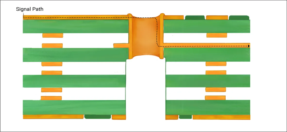
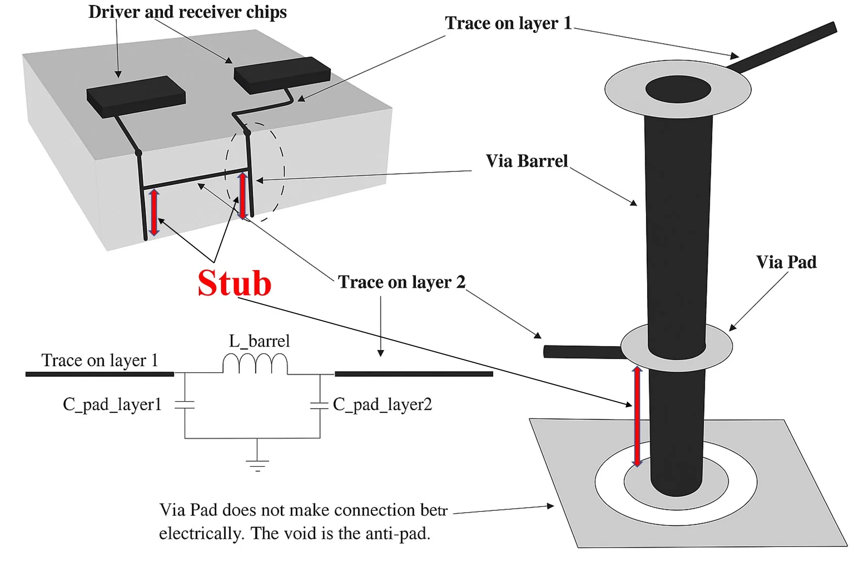
Controlled depth drilling involves creating a through-hole via first, followed by a secondary drill from one side using a larger bit to reach a precise depth. This removes the conductive stub beyond the signal layer, preventing signal reflections and crosstalk in multilayer boards. In high-frequency designs, stubs act as antennas, causing impedance discontinuities and insertion loss. Without proper back drilling, signal integrity issues degrade performance, particularly above multi-Gbps rates. Manufacturers prioritize this method for boards thicker than standard, where blind or buried vias alone fall short. Its relevance grows with denser interconnects, demanding tight tolerances for viable production.
The process demands coordination between design files, stack-up data, and drilling equipment. Depth accuracy typically targets within specific margins to avoid over-penetration or under-drilling. Industry practices emphasize verifying panel flatness and material consistency beforehand. Effective implementation directly impacts yield rates in production runs. Engineers benefit from recognizing its role in overall PCB quality control.
Technical Principles Behind Common Controlled Depth Drilling Problems
Several mechanisms contribute to controlled depth drilling problems during execution. Primary among them is depth control inaccuracy, where the drill either fails to reach the target or penetrates too far. Variations in laminate thickness, panel warpage, or inconsistent entry materials disrupt Z-axis precision. Machine spindle runout or worn sensors exacerbate these deviations, leading to uneven stub removal across panels. Resulting stubs maintain electrical discontinuities, fostering PCB drilling defects observable in cross-sections.
Misalignment ranks as another prevalent issue in back drilling troubleshooting. The secondary drill bit, oversized by a margin relative to the original via, must center precisely on the plated barrel. Registration errors from panel shifts, drill wander, or inadequate fiducials cause offset drilling. This produces crescent-shaped remnants or damages adjacent copper. Thermal expansion differences between layers compound positioning challenges during multi-panel stacks. Factory observations link such defects to rushed setups without pilot verification.
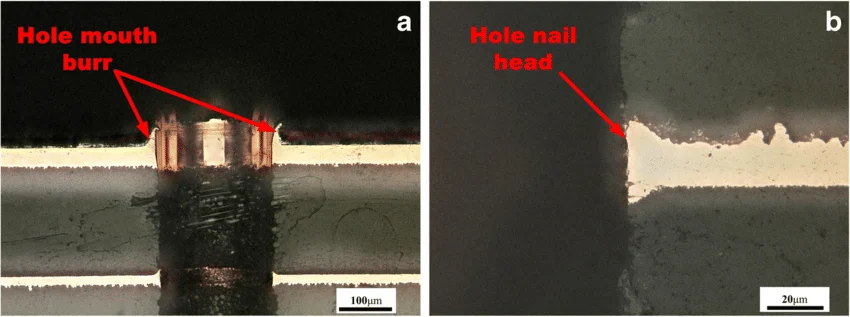
Hole wall quality often suffers from burrs, roughness, or carbonization. Excessive heat from high feed rates or dull bits smears resin, adhering to copper walls. Burrs form when chips fail to evacuate properly, scratching surfaces during withdrawal. These irregularities hinder subsequent plating adhesion, inviting voids or cracks. IPC-A-600 guidelines define acceptability criteria for hole walls, classifying roughness levels that affect reliability. Addressing these requires balanced parameters tailored to material types.
Over-drilling poses risks to inner layers, manifesting as breakout defects. When depth exceeds specifications, the drill severs traces or lands on sensitive planes. Stack-up misinterpretation or absent break-ring cues in artwork contribute here. Such errors trigger opens in nets, detectable via flying probe tests. Signal paths weaken, amplifying PCB manufacturing errors in high-density designs. Preventive modeling simulates paths to flag vulnerabilities early.
Impacts of Drilling Defects on Signal Integrity
PCB drilling defects from controlled depth drilling directly undermine signal integrity issues. Residual stubs reflect signals, introducing jitter and eye closure in high-speed links. Incomplete removal leaves capacitive loads, shifting characteristic impedance. Crosstalk intensifies between adjacent vias lacking clearance. Time-domain reflectometry reveals these anomalies post-fabrication. Engineers must correlate defects to performance metrics during validation.
Plating complications arise post-drilling, where rough walls promote poor copper deposition. Voids or thin plating create high-resistance paths, prone to electromigration. Desmear processes struggle with carbonized residue, leading to inconsistent etch-back. These translate to intermittent failures under thermal cycling. Reliability testing per IPC-6012 standards verifies barrel pull strength. Factory data underscores how early defect correction preserves margins.
Warpage influences all defects, as bowed panels skew depth measurements. Material anisotropy or asymmetric drilling sequences induce stresses. Thicker cores amplify this, necessitating fixturing. Resultant defects cluster in panel corners, complicating yield analysis. Maintaining flatness below thresholds ensures uniform results.
Practical Troubleshooting and Best Practices for Back Drilling
Back drilling troubleshooting starts with design verification. Specify drill depths with tolerances, incorporating margins for material variance. Use break-rings or target depths tied to layer pairs in stack-up notes. Simulate via stubs in signal models to justify locations. Allocate routing channels for oversized drills, typically 0.10 to 0.15 mm larger. Clear documentation prevents interpretation errors at fabrication.
In production, calibrate machines using depth sensors and foil entry materials. Conduct pilot runs on scrap panels to dial feed speeds and rotations. Monitor spindle loads to detect bit wear early. Employ vision systems for alignment checks pre-drill. Post-drill, perform automated optical inspections for burrs and offsets. Cross-section samples confirm stub lengths across zones.
Desmear optimization tackles smear effectively. Plasma or chemical treatments remove residue without over-etching. Adjust permanganate cycles based on drill heat history. Peck drilling aids chip evacuation in deep holes. These steps align with IPC-DR-572 recommendations for mechanical drilling parameters. Consistent application boosts first-pass yields.
For breakout prevention, integrate Z-axis stops or conductive foils signaling target depth. Layer spacing should exceed drill oversize plus breakthrough margin. Electrical continuity tests post-plating flag damages swiftly. Rework via blind fills proves feasible for isolated cases. Training operators on anomaly recognition sustains quality. Collaborative reviews between design and fab teams refine processes iteratively.
Conclusion
Troubleshooting controlled depth drilling problems demands precision across design, fabrication, and inspection. Common PCB drilling defects like misalignment, depth errors, and wall irregularities stem from controllable factors such as calibration and parameters. Prioritizing back drilling troubleshooting mitigates signal integrity issues, ensuring robust high-speed performance. Adhering to standards like IPC-A-600 and IPC-6012 fortifies outcomes. Engineers gain reliability by integrating best practices into workflows. Ultimately, these efforts elevate PCB manufacturing quality, reducing errors and enhancing product longevity.
FAQs
Q1: What are the main causes of misalignment in controlled depth drilling problems?
A1: Misalignment occurs due to registration shifts in panels, drill wander from bit runout, or imprecise fiducials. Thermal effects during processing alter coordinates between initial and back drills. Inadequate artwork scaling compounds issues in multi-panel arrays. Factory troubleshooting involves vision alignment and pilot verification to center the larger bit accurately on the via barrel. This ensures complete stub removal without offsets.
Q2: How do you troubleshoot depth inaccuracies in back drilling?
A2: Verify stack-up thicknesses and use depth-sensing spindles for real-time control. Entry foils or break-rings provide tactile stops. Calibrate against known panels, adjusting for warpage via vacuum fixturing. Cross-section analysis quantifies residuals post-process. Optimizing feed and peck cycles prevents over-drill breakouts. Consistent parameters per IPC-DR-572 guidelines maintain tolerances.
Q3: What role do hole wall burrs play in PCB drilling defects?
A3: Burrs from poor chip evacuation scratch walls, impairing plating adhesion and inviting voids. They arise at high feeds or dull bits, especially in resin-rich materials. Burrs elevate roughness beyond acceptability, per IPC-A-600 criteria. Deburring brushes or optimized withdrawal mitigate them. Smooth walls support reliable barrel integrity under stress.
Q4: Can signal integrity issues arise from incomplete back drilling troubleshooting?
A4: Yes, lingering stubs cause reflections and impedance mismatches, degrading eye patterns. Crosstalk rises without stub isolation. TDR measurements confirm fixes. Proper depth control eliminates these, preserving margins for high-speed signals.
References
IPC-A-600K — Acceptability of Printed Boards. IPC, 2020
IPC-6012E — Qualification and Performance Specification for Rigid Printed Boards. IPC, 2017
IPC-DR-572A — Design and Assembly Process Implementation for Homogeneous Copper Plating of PCBs. IPC, 2016


