 ALLPCB


Introduction
Printed circuit boards form the backbone of modern electronics, supporting complex circuits in everything from consumer devices to industrial systems. Despite advances in materials and processes, PCB failure remains a persistent challenge for engineers, often traced back to subtle design and manufacturing issues. One such overlooked culprit is uneven copper distribution, which quietly undermines board integrity over time. This imbalance triggers mechanical stresses that manifest as warpage, delamination, and electrical inconsistencies, leading to premature pcb failure. Electric engineers must recognize these hidden dangers to enhance reliability and reduce costly rework. Understanding the principles behind uneven copper distribution empowers better design decisions from the outset.
What Is Uneven Copper Distribution and Why It Matters
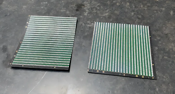
Uneven copper distribution occurs when copper traces, planes, and fills vary significantly in density or weight across a PCB's layers or within individual layers. This imbalance can arise from concentrated routing on one side or sparse areas lacking compensatory features. In multilayer boards, it often stems from asymmetric stackups where outer layers carry heavy power planes while inner signal layers remain light. Such disparities disrupt the board's structural harmony, amplifying pcb problems during thermal cycling and mechanical handling.
The relevance intensifies in high-reliability applications, where even minor deviations compromise performance. Uneven copper distribution directly contributes to pcb failure modes like excessive bow and twist, which exceed acceptability limits defined in IPC-A-600. These deformations hinder surface-mount technology assembly, causing component misalignment and solder joint defects. Over time, they accelerate fatigue in vias and traces, shortening operational life. For electric engineers, addressing copper balancing early prevents field returns and ensures compliance with qualification standards such as IPC-6012E. Ignoring it invites cascading issues from fabrication to end-use.
Root Causes of Uneven Copper Distribution
PCB design flaws represent the primary origin of uneven copper distribution, where engineers prioritize functionality over symmetry. Dense trace clusters for high-speed signals on one layer contrast with open ground planes elsewhere, creating density gradients up to 50% or more. Asymmetric component placement exacerbates this, as power delivery networks dominate one half of the board. Manufacturing tolerances in etching and plating then amplify these flaws, with uneven etchant flow leading to over-etching in sparse regions.
Fabrication processes introduce additional variability through panel-level effects. During electroplating, low-copper areas receive thicker deposits as current concentrates there, inverting the intended balance. Lamination under heat and pressure warps the core toward copper-heavy sides due to differential shrinkage. These combined factors result in persistent pcb problems, including inconsistent impedance and thermal hotspots. Electric engineers must audit layer densities during layout reviews to mitigate such risks proactively.
Engineering Mechanisms Behind PCB Failures
The core mechanism linking uneven copper distribution to pcb failure lies in mismatched coefficients of thermal expansion between copper and the laminate substrate. Copper expands roughly four times more than typical FR-4 during reflow or operation, generating internal stresses in imbalanced areas. These stresses accumulate over thermal cycles, causing micro-cracks at interfaces and progressive delamination. Warpage emerges as the board bows toward the lighter copper side, violating flatness tolerances critical for automated assembly.
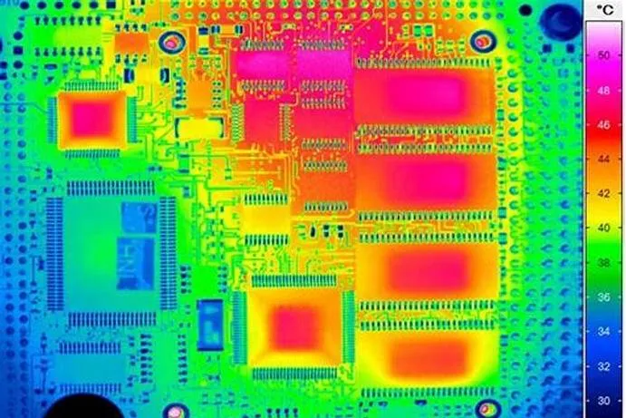
Electrically, uneven distribution skews signal propagation, introducing crosstalk and attenuation variations. High-current paths overheat disproportionately, degrading nearby dielectrics and vias. Mechanical vulnerabilities compound this, as twisted boards experience higher peel strength failures under vibration. J-STD-020 provides guidelines for handling such sensitivities, but prevention at the design stage remains essential. Engineers observe these effects most acutely in high-layer-count boards subjected to harsh environments.
Detecting Uneven Copper Distribution in Practice
Early detection requires systematic checks during design verification and incoming inspection. Layer stackup reviews should quantify copper coverage per signal layer, flagging deviations beyond 20% from the average. Cross-section analysis post-prototype reveals plating uniformity, while automated optical inspection scans for etch inconsistencies. Warpage measurement using straight edges or laser profilometers quantifies bow and twist against baseline panels.
In production, fixture-based testing simulates assembly stresses, exposing latent pcb design flaws. Thermal imaging during powered operation highlights hotspots from imbalanced planes. Data logging from these methods correlates directly with field pcb failure rates, guiding iterative improvements. Electric engineers benefit from integrating these into design for manufacturability workflows.
Best Practices for Copper Balancing
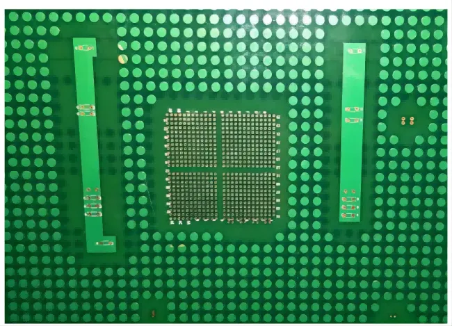
Copper balancing starts with symmetric stackup planning, mirroring copper densities between paired layers from the core outward. For instance, if layer 1 features 60% fill for power, layer 16 should match in a 16-layer board. Designers employ copper thieving patterns, small isolated pads in open areas, to equalize density without altering electrical performance. These patterns, spaced at least 0.5 mm from traces, ensure uniform etching and plating.
Hatch or grid fills provide finer control, achieving 40-60% coverage in ground planes while minimizing parasitic capacitance. Simulation tools model warpage by inputting layer densities and material properties, predicting deformations before fabrication. Manufacturing partners apply panel-level balancing during imaging, adding global thieving frames. Adhering to IPC-2221 design guidelines reinforces these practices, promoting robust boards.
During routing, distribute traces evenly and avoid large voids exceeding 10% of layer area. Core selection with matched CTE materials further stabilizes the stack. Post-lamination baking relieves residual stresses, while controlled cooling prevents re-warping. These layered strategies collectively minimize uneven copper distribution risks.
Troubleshooting Common PCB Problems from Imbalance
When pcb failure occurs, engineers first assess warpage magnitude against IPC-A-600 criteria. Excessive bow prompts layer-by-layer copper audits via X-ray or ultrasound. Delamination signals CTE mismatch, confirmed by cross-section microscopy revealing voids at copper-laminate interfaces. Solder joint issues trace to uneven reflow, mitigated by profile adjustments.
Vibration testing isolates mechanical weaknesses, with failure analysis pinpointing trace lifts from stress concentrations. Corrective actions include redesign with enhanced balancing and material swaps for better compliance. Documenting these insights refines future designs, reducing recurrence.
Conclusion
Uneven copper distribution stands as a stealthy architect of pcb failure, driving warpage, electrical anomalies, and reliability gaps through thermal and mechanical stresses. Electric engineers armed with copper balancing techniques, from thieving to symmetric layouts, can avert these pitfalls effectively. Integrating standards like IPC-6012E into workflows ensures qualification success and long-term performance. Prioritizing balance transforms potential pcb problems into strengths, yielding durable boards for demanding applications. Proactive design remains the ultimate safeguard against these hidden dangers.
FAQs
Q1: How does uneven copper distribution cause PCB warpage?
A1: Uneven copper distribution creates differential thermal expansion during heating, as copper-heavy areas expand more than sparse ones. This generates bending stresses, bowing the board toward lighter regions. Manufacturers measure this against IPC-A-600 limits to reject non-conforming panels. Copper balancing through thieving prevents such pcb failure by equalizing layer densities.
Q2: What are the main PCB design flaws leading to uneven copper?
A2: Key flaws include asymmetric trace routing, unbalanced power planes, and ignoring layer pairing in stackups. Large empty areas invite plating variations, worsening imbalance. Engineers counter this with density audits and fill patterns. Proper copper balancing integrates seamlessly into design flows for reliable outcomes.
Q3: How can engineers implement copper balancing effectively?
A3: Start by mirroring copper coverage across symmetric layers, targeting 40-60% density uniformity. Add thieving patterns in voids and simulate warpage pre-fabrication. Collaborate with fabricators for panel balancing. These steps address uneven copper distribution, minimizing pcb problems per IPC guidelines.
Q4: Why is copper balancing critical for multilayer PCBs?
A4: Multilayer boards amplify stresses from uneven copper distribution due to compounded layer interactions. Imbalance leads to delamination and via failures under thermal cycling. Balancing ensures flatness for assembly and sustains signal integrity. It directly combats common pcb failure modes in high-density designs.
References
IPC-6012E — Qualification and Performance Specification for Rigid Printed Boards. IPC, 2017
IPC-A-600K — Acceptability of Printed Boards. IPC, 2020
J-STD-020E — Moisture/Reflow Sensitivity Classification. JEDEC, 2014


