ALLPCB


Surface finish on SMT stencils plays a direct role in how effectively solder paste transfers from the stencil apertures to the PCB pads during printing. Engineers working in PCB assembly often focus on aperture design and thickness, yet the condition of the aperture walls can determine whether paste releases cleanly or adheres to the stencil. Poor release leads to insufficient solder volume, bridging, or inconsistent deposits that affect downstream reflow and joint reliability. Selecting an appropriate stencil surface finish helps maintain consistent paste transfer efficiency across production runs.
Why Stencil Surface Finish Matters in SMT Assembly
The surface finish inside stencil apertures influences solder paste adhesion and the overall transfer ratio. When paste sticks to rough or high-energy walls, less material reaches the pads, reducing deposit volume and increasing the risk of open joints or weak connections. In high-volume manufacturing, even small variations in transfer efficiency can accumulate into significant yield losses. Practical experience shows that optimizing the stencil surface finish supports more stable printing processes, especially with fine-pitch components or dense layouts. This factor becomes particularly relevant when troubleshooting recurring print defects that persist despite correct aperture sizing.
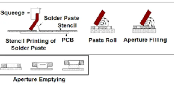
Industry guidelines such as those in IPC-7525 address stencil design parameters that interact with surface conditions to achieve reliable paste deposition.
Technical Principles of Surface Finish Effects on Paste Release
Solder paste release depends on the balance between the forces pulling paste onto the pad and those holding it against the aperture walls. Rough surfaces increase mechanical interlocking and surface area contact, raising adhesion. Smoother finishes reduce these interactions, allowing the paste to separate more completely when the stencil lifts. Surface energy also plays a part; lower-energy coatings discourage wetting and sticking by the flux and solder particles.
Related Reading: Nano-Coating Stencils: Enhancing Solder Paste Release for High-Density PCBs
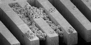
Engineers observe that aperture wall texture affects both initial print quality and long-term performance as the stencil accumulates residue. Over multiple prints, minor surface irregularities can trap particles or dried flux, further degrading release characteristics. Consistent surface finish therefore supports repeatable results across shifts and batches. These mechanisms explain why finish selection often forms part of root-cause analysis when transfer efficiency falls below expectations.
Electropolishing and Nano-Coating Stencils: Mechanisms and Benefits
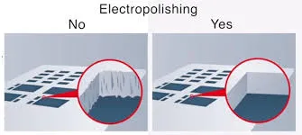
Electropolishing removes microscopic peaks from laser-cut or etched aperture walls through an electrochemical process, producing smoother surfaces that lower friction and solder paste adhesion. The result is improved paste transfer, particularly for smaller apertures where the wall-to-opening area ratio is critical. Benefits include reduced residue buildup and easier cleaning between prints.
Nano-coating stencils apply thin layers that modify surface energy without altering aperture dimensions. These coatings create a barrier that limits direct contact between paste and base metal, further enhancing release while protecting against oxidation. In practice, combining electropolishing with nano-coatings often delivers the highest transfer efficiency for challenging designs. Engineers note that such finishes maintain performance longer under production conditions compared with untreated stencils.
Related Reading: Nano Coatings for Stencils: Enhancing Aperture Performance and Solder Paste Transfer
Best Practices for Selecting and Maintaining Stencil Surface Finishes
When specifying stencils, evaluate the expected aperture sizes and component pitches first, then match the surface finish to the required transfer performance. For fine features, electropolished or nano-coated options typically provide measurable improvements in paste release consistency. Maintenance routines should include regular inspection for coating wear or surface degradation that could reintroduce adhesion issues.
Proper storage and cleaning protocols help preserve the finish; aggressive solvents or mechanical scrubbing can damage coatings and negate their benefits. Documentation of stencil condition after each use supports trend analysis and timely reconditioning or replacement decisions. These steps integrate into broader process control efforts aimed at stable SMT output.
Troubleshooting Common Paste Release Issues Related to Surface Finish
When paste transfer falls short, surface finish should be examined alongside other variables such as squeegee pressure and paste rheology. Visible residue on aperture walls after printing often points to inadequate smoothness or coating condition. In such cases, switching to or restoring an electropolished or nano-coated stencil frequently restores acceptable transfer ratios without redesigning apertures.
Engineers also check for progressive degradation over the stencil's life; initial performance may be good, yet wear can increase adhesion later. Comparing prints from new versus used stencils under identical conditions isolates finish-related effects. Addressing these issues early prevents escalation into broader assembly defects.
Conclusion
Stencil surface finish directly affects solder paste adhesion and transfer efficiency in SMT processes. Electropolishing and nano-coating stencils offer practical ways to improve release by reducing wall roughness and surface energy. When combined with sound design practices and maintenance, these finishes contribute to more consistent printing results and fewer defects. Engineers benefit from evaluating finish options as part of routine process optimization rather than treating them as secondary considerations.
FAQs
Q1: How does stencil surface finish influence improving paste transfer during SMT printing?
A1: Surface finish determines how much solder paste adheres to aperture walls versus transferring to the PCB. Smoother finishes from electropolishing or nano-coating stencils reduce adhesion, allowing higher transfer efficiency. This effect becomes more pronounced with smaller apertures where wall area is relatively large. Consistent finish quality supports repeatable deposit volumes across production.
Q2: What are the main electropolishing benefits for SMT stencil performance?
A2: Electropolishing smooths aperture walls by removing microscopic irregularities, which lowers friction and solder paste adhesion. The process improves paste release without changing aperture dimensions. It also reduces residue accumulation, simplifying cleaning and extending effective stencil life under normal use.
Q3: When should nano-coating stencils be considered over standard finishes?
A3: Nano-coating stencils are useful when standard finishes show insufficient release, especially in fine-pitch or high-density applications. The coatings lower surface energy to minimize paste sticking while protecting the base material. They work well in combination with electropolishing for demanding printing conditions.
Q4: How can engineers troubleshoot solder paste adhesion problems linked to stencil surface finish?
A4: Start by inspecting aperture walls for residue or visible roughness after printing. Compare transfer results between stencils with different finishes under the same process settings. Restoring or upgrading to electropolished or nano-coated surfaces often resolves persistent adhesion without altering other parameters.
References
IPC-7525C — Stencil Design Guidelines. IPC
IPC J-STD-005B — Requirements for Solder Pastes. IPC & JEDEC
IPC-A-600K — Acceptability of Printed Boards. IPC, 2020