 ALLPCB


Why Advanced Materials Matter for Aerospace PCBs
Aerospace systems demand printed circuit boards that maintain reliable operation under extreme conditions. Advanced materials play a central role in meeting these requirements by improving thermal stability, electrical performance, and mechanical durability. Engineers select high-performance PCB substrates to address the unique challenges of vibration, temperature cycling, and radiation exposure typical in aircraft and spacecraft environments. These material choices directly influence signal integrity and long-term reliability in mission-critical applications.
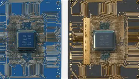
Aerospace PCB advanced materials extend beyond conventional FR-4 laminates to include specialized polymers and composites. High-performance PCB substrates such as polyimide and fluoropolymer-based materials provide the necessary combination of low dielectric loss and high glass transition temperatures. Conductive inks PCB solutions enable finer trace geometries and flexible interconnects that reduce weight while preserving conductivity. Biodegradable PCBs remain an emerging consideration, though their adoption in aerospace stays limited due to stringent performance and qualification demands.
Engineers evaluate these materials against operational envelopes that include rapid temperature changes and mechanical stress. The selection process balances electrical properties with thermal expansion characteristics to minimize warpage and delamination risks. Industry standards guide qualification testing to ensure consistent performance across production batches.
Technical Principles of Material Performance
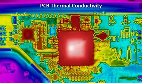
Material selection begins with understanding dielectric constant and dissipation factor, which govern signal propagation speed and loss in high-frequency circuits. Aerospace PCB electrical properties improve when substrates exhibit stable values across wide temperature ranges. Thermal conductivity becomes equally important, as heat generated by power components must dissipate efficiently to prevent localized overheating.
High-performance PCB substrates often incorporate ceramic fillers or specialized resins to achieve these characteristics. Conductive inks PCB formulations allow additive manufacturing techniques that reduce material waste and enable three-dimensional routing. Thermal expansion coefficients must align closely with attached components to avoid stress during temperature excursions. These mechanisms work together to maintain electrical continuity and mechanical integrity throughout the product lifecycle.
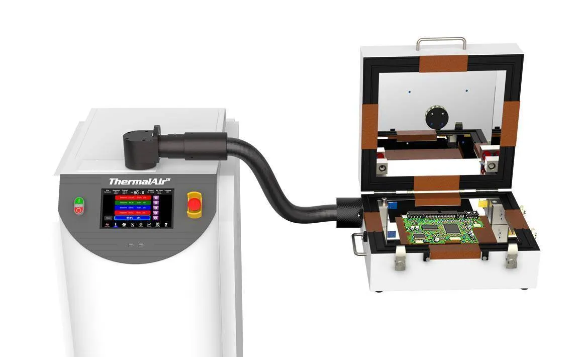
Standards such as IPC-6012E establish qualification requirements for rigid printed boards used in demanding applications. Testing protocols verify that material properties remain within specified limits after exposure to environmental stresses.
Enhancing Thermal and Electrical Properties
Aerospace PCB thermal properties receive particular attention because operating temperatures can range from cryogenic conditions to several hundred degrees Celsius. Materials with low coefficients of thermal expansion and high thermal conductivity help maintain dimensional stability. Engineers often combine multiple layers with different thermal characteristics to optimize heat flow paths.
Electrical performance benefits from substrates that support controlled impedance routing and low-loss signal transmission. Conductive inks PCB technology supports the creation of fine-line circuits with consistent resistivity. These improvements translate into higher data rates and reduced power consumption in avionics and communication systems.
Practical Considerations in Material Selection and Design
Design teams follow structured evaluation processes when specifying aerospace PCB advanced materials. Finite element analysis helps predict stress distribution and identify potential failure points before prototyping. Material datasheets provide baseline values, yet actual performance requires verification through standardized testing.
Best practices include selecting substrates compatible with assembly processes such as soldering and underfill application. Trace layout accounts for coefficient of thermal expansion mismatch to reduce fatigue in interconnects. Documentation of material lot traceability supports quality audits and failure analysis when needed.
Standards such as IPC-A-600K define acceptability criteria for printed boards, helping teams maintain consistent quality levels during manufacturing.
Sustainability and Emerging Material Options
Biodegradable PCBs represent an area of ongoing research aimed at reducing environmental impact at end of life. Current aerospace requirements prioritize reliability and long service life, which limits immediate adoption of these materials. Engineers continue to explore hybrid approaches that incorporate sustainable elements without compromising performance.
Material suppliers develop formulations that balance regulatory compliance with functional demands. Lifecycle assessments guide decisions on whether biodegradable options can meet the rigorous qualification standards required for flight hardware.
Conclusion
Advanced materials continue to expand the performance envelope of aerospace PCBs by delivering improved thermal management and electrical characteristics. High-performance PCB substrates, conductive inks PCB technologies, and careful attention to aerospace PCB thermal properties and aerospace PCB electrical properties enable reliable operation in challenging environments. Structured design practices aligned with established industry standards support consistent results across programs. Continued material development will further enhance capabilities while addressing emerging sustainability considerations.
FAQs
Q1: How do high-performance PCB substrates improve aerospace PCB electrical properties?
A1: High-performance PCB substrates maintain stable dielectric constants and low dissipation factors across temperature extremes. This stability supports consistent signal integrity and controlled impedance in high-frequency circuits used in avionics and communication systems. Engineers select these materials to minimize losses that would otherwise degrade performance during flight operations.
Q2: What role do conductive inks PCB play in modern aerospace designs?
A2: Conductive inks PCB enable additive deposition of circuit traces, allowing finer features and reduced weight compared with traditional subtractive processes. They support flexible and three-dimensional interconnects that accommodate complex packaging requirements. These inks maintain conductivity while meeting the mechanical and environmental demands of aerospace applications.
Q3: Are biodegradable PCBs suitable for aerospace PCB advanced materials applications?
A3: Biodegradable PCBs remain under evaluation for aerospace use because current formulations may not yet satisfy long-term reliability and qualification requirements. Research focuses on achieving necessary thermal and electrical properties while meeting end-of-life environmental goals. Most flight hardware continues to rely on established high-performance substrates that prioritize durability.
Q4: How do aerospace PCB thermal properties influence material selection?
A4: Aerospace PCB thermal properties such as conductivity and expansion coefficients determine how well a board manages heat and maintains dimensional stability. Materials with matched expansion rates reduce stress on components during temperature cycling. Engineers evaluate these characteristics to prevent delamination and ensure reliable operation across the expected thermal range.


