 ALLPCB


Introduction
In printed circuit board design, the choice of PCB material profoundly influences trace routing strategies and overall signal performance. Electric engineers must consider how the dielectric properties of the PCB material dictate impedance control, signal propagation speed, and loss characteristics during layout. Selecting the appropriate dielectric ensures that traces can be routed efficiently without compromising high-speed signal integrity. This article explores the critical interplay between PCB material selections and trace routing decisions. By understanding PCB dielectric constant and PCB loss tangent, designers can optimize routing density and minimize crosstalk in multilayer boards. Proper material selection aligns with industry standards to support reliable performance across frequencies.
Understanding PCB Dielectrics and Key Properties
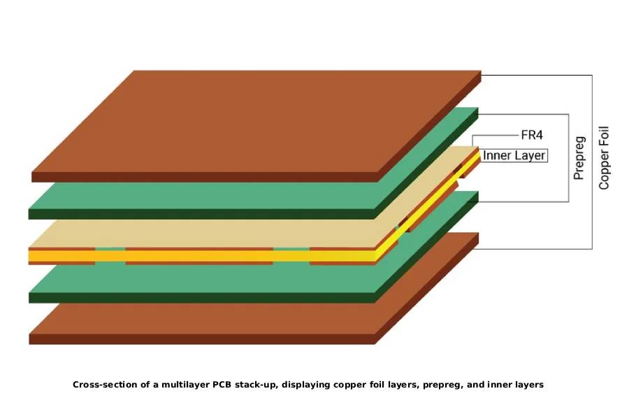
PCB dielectrics form the insulating core between conductive traces, directly impacting electrical behavior. The PCB dielectric constant, often denoted as Dk or εr, quantifies the material's ability to store electrical energy relative to air. Materials with lower Dk values permit faster signal propagation, as the effective velocity is inversely proportional to the square root of Dk. Conversely, higher Dk materials increase capacitance per unit length, which can alter trace impedance. PCB loss tangent, or Df, measures the dissipative losses in the dielectric, converting signal energy into heat. Engineers evaluate these properties during material selection to match routing requirements.
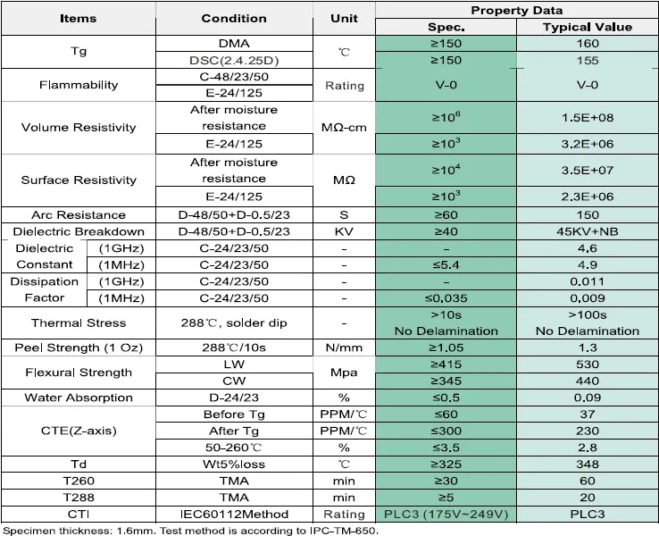
Standards like IPC-4101E specify qualification criteria for base materials, including consistent Dk and Df values across batches. These properties vary with frequency, temperature, and moisture, necessitating characterization over operational ranges. For instance, FR-4 resins typically exhibit Dk around 4.0 to 4.5 at 1 GHz, while advanced low-loss materials offer lower values. Trace routing benefits from stable dielectrics that maintain predictable electrical parameters. Selecting materials per these guidelines prevents deviations that could necessitate redesigns.
How PCB Dielectric Constant Affects Trace Routing
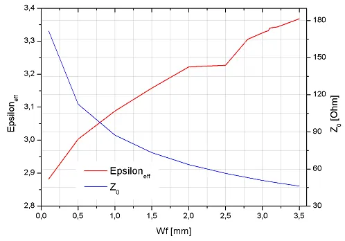
The PCB dielectric constant governs characteristic impedance in transmission lines like microstrips and striplines. Impedance Z0 is calculated as Z0 = (87 / sqrt(Dk + 1.41)) * ln(5.98h / (0.8w + t)) for microstrips, where h is dielectric height, w is trace width, and t is thickness. Higher Dk reduces Z0 for fixed geometry, requiring wider traces or thicker dielectrics to compensate, which impacts routing density. In high-speed designs, low-Dk materials enable tighter spacing by reducing capacitive coupling between adjacent traces. This allows more aggressive routing in dense layouts without excessive crosstalk.
Engineers must account for Dk variation across the board due to glass weave patterns in woven reinforcements. Non-uniform Dk leads to impedance mismatches along traces, causing reflections and signal distortion. Routing strategies often involve aligning traces with uniform weave regions or using spread glass for homogeneity. Multilayer boards amplify these effects, as inter-layer dielectrics influence via transitions. Optimizing Dk selection thus streamlines trace routing while preserving signal quality.
The Role of PCB Loss Tangent in Signal Integrity
PCB loss tangent quantifies dielectric inefficiency, where tan δ = ε'' / ε', with ε'' representing the lossy component of permittivity. At microwave frequencies, high Df causes insertion loss, attenuating signals over long traces and necessitating repeaters or redesigns. Low-loss dielectrics with Df below 0.005 minimize attenuation, supporting routing of high-frequency signals like RF or 100 Gbps Ethernet. Conductor losses from copper also interact with Df, but dielectric contribution dominates above 10 GHz.
In trace routing, high Df exacerbates skin effect losses, broadening pulse rise times and introducing jitter. Designers route sensitive traces on low-Df layers, avoiding bends that increase path length. IPC-2221 provides design guidelines for material selection to mitigate these losses in controlled impedance structures. Balancing Df with cost enables practical high-speed routing without excessive power consumption from signal regeneration.
Factors Influencing Dielectric Selection for Trace Routing
Frequency range dictates primary dielectric requirements; low-speed designs tolerate standard FR-4, while GHz signals demand low-Dk, low-Df alternatives. Thermal expansion mismatch between dielectric and copper affects via reliability, influencing routing near connectors. Moisture absorption alters Dk and Df, so low-absorption materials suit humid environments. Cost, availability, and process compatibility further constrain choices.
Routing density benefits from thinner dielectrics with low Dk, enabling finer lines per IPC class definitions. However, thin layers risk mechanical fragility, requiring balanced stackups. Engineers simulate stackups to predict impedance tolerances within 10%, adjusting routing accordingly. Hybrid materials combining cores and prepregs offer tailored properties for complex routing.
Best Practices for Selecting and Routing with PCB Materials
Begin with stackup planning, specifying Dk and Df targets based on impedance specs. Use field solvers to model trace geometries, iterating widths and spacings. Reference IPC-4101E for material qualification to ensure reproducibility. Route high-speed traces as differential pairs on uniform dielectric regions, minimizing length mismatches.
Implement ground planes adjacent to signal layers to stabilize impedance and reduce radiation. Avoid splitting planes under traces to prevent impedance discontinuities. For high-density interconnects, select materials with tight Dk tolerance below 1%. Post-layout verification confirms routing meets loss budgets. These practices optimize PCB material utilization for efficient trace routing.
Practical Insights from High-Speed Design Challenges
Consider a multilayer board for data center switches, where 56 Gbps PAM4 signals demand low-loss routing. Standard FR-4's Df causes 20 dB loss per inch at 28 GHz, forcing shorter traces and more vias. Switching to low-Dk prepregs reduces loss by half, allowing denser routing with fewer layers. Engineers adjusted trace widths from 4 mils to 3 mils, fitting 20% more channels.
Troubleshooting impedance deviations often reveals Df-induced skew in length-matched buses. Fabricators measure Dk per IPC-TM-650 methods, feeding data back for rerouting. These scenarios underscore dielectric selection's role in feasible layouts.
Conclusion
PCB material choices, particularly dielectric constant and loss tangent, fundamentally shape trace routing outcomes. Low-Dk, low-Df materials enable higher densities and better signal integrity in electric engineering applications. Adhering to standards like IPC-2221 and IPC-4101E ensures designs meet performance without fabrication surprises. Engineers should prioritize simulation and material characterization early. This approach yields robust, routable boards ready for high-speed demands. Future trends toward terahertz signals will amplify the need for advanced dielectrics.
FAQs
Q1: What is the PCB dielectric constant and why does it matter for trace routing?
A1: The PCB dielectric constant (Dk) measures a material's permittivity, influencing capacitance and impedance in traces. Higher Dk lowers characteristic impedance, requiring wider traces that reduce routing density. For high-speed designs, low Dk around 3.0 to 3.5 supports tighter spacings and faster propagation. Engineers select based on frequency to control crosstalk and reflections.
Q2: How does PCB loss tangent impact high-frequency trace performance?
A2: PCB loss tangent (Df) indicates dielectric energy dissipation as heat, causing signal attenuation in long traces. At GHz frequencies, higher Df degrades eye diagrams and bit error rates. Low-Df materials preserve amplitude for routing extended buses. Pair with smooth copper to minimize total loss.
Q3: Which PCB material properties should electric engineers prioritize for impedance-controlled routing?
A3: Prioritize stable PCB dielectric constant and low PCB loss tangent for predictable impedance. Uniform Dk across weave prevents mismatches; Df below 0.005 suits RF routing. Consider CTE for reliability. Simulate stackups per design standards for optimal trace widths.
Q4: Can standard FR-4 handle advanced trace routing in high-speed PCBs?
A4: Standard FR-4 with Dk ~4.2 and Df ~0.02 works for up to 10 Gbps but struggles beyond due to high loss tangent. For denser, faster routing, use low-loss variants or hybrids. Balance with cost for production.
References
IPC-4101E — Specification for Base Materials for Rigid and Multilayer Printed Boards. IPC, 2017
IPC-2221B — Generic Standard on Printed Board Design. IPC, 2012
IPC-TM-650 — Test Methods Manual. IPC, 2020


