ALLPCB


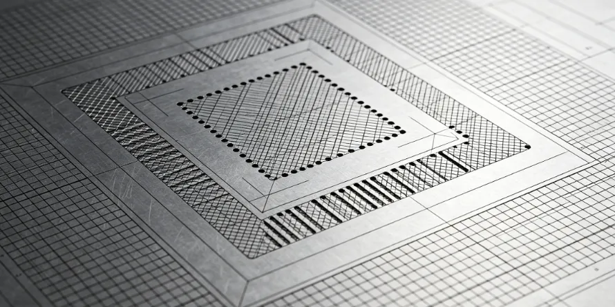
Laser cut stencils play a central role in surface mount technology assembly by controlling the precise amount of solder paste applied to printed circuit board pads. The thickness of these stencils directly influences the volume of paste deposited during the printing process. Engineers and assembly teams must understand this relationship to achieve reliable solder joints while minimizing defects such as bridging or insufficient wetting. Variations in stencil thickness affect both the quantity and the consistency of solder paste transfer, which in turn impacts overall process yield and product reliability. Proper selection supports consistent results across different component types and board designs.
Why Stencil Thickness Matters in Solder Paste Application
Stencil thickness determines how much solder paste fills the apertures and transfers onto the board during printing. Thicker stencils generally allow greater paste volume, which can benefit larger components that require more solder for mechanical strength and thermal performance. Conversely, thinner stencils reduce the risk of excess paste that might cause short circuits between closely spaced leads. The choice of thickness must balance the needs of fine-pitch devices against those of larger components on the same assembly. Industry practices emphasize evaluating stencil thickness early in the design phase to avoid costly rework later in production.
Technical Principles of Solder Paste Deposition
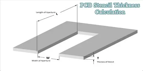
Solder paste deposition relies on the interaction between stencil apertures, squeegee pressure, and paste rheology. When the stencil is placed on the board, paste is forced through the openings by the moving squeegee blade. The volume released depends on aperture area multiplied by stencil thickness, adjusted for release efficiency. Thicker stencils increase the potential volume but can also raise the chance of paste sticking inside the apertures if aspect ratios are not optimized. Laser cutting produces smooth, vertical walls that improve paste release compared with older etching methods, yet thickness remains the dominant variable controlling deposited volume.
Engineers analyze stencil thickness versus solder volume by considering the area ratio and aspect ratio of each aperture. These ratios help predict whether paste will release cleanly or remain trapped. In practice, the relationship between thickness and final solder joint height follows predictable patterns when process parameters stay constant. Variations in board flatness or paste viscosity can modify the outcome, requiring adjustments during setup. Consistent monitoring of printed deposits helps maintain control over the process.
Related Reading: Decoding Stencil Thickness: A Comprehensive Guide for PCB Assembly Success
Practical Guidance for Selecting and Using Stencils
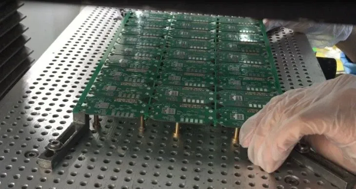
Assembly teams often begin by reviewing the component mix on a board to guide stencil thickness decisions. Boards populated with a wide range of part sizes benefit from thickness choices that accommodate both fine features and larger pads without compromising either. Laser cut stencils allow precise aperture customization that complements thickness selection. Regular inspection of stencils for wear or deformation ensures that thickness remains uniform across the working area throughout production runs.
Troubleshooting begins with examining printed paste deposits for volume consistency. Insufficient volume may indicate that the current thickness is too low for certain apertures, while bridging often points to excessive volume from a thicker stencil. Adjusting print parameters such as speed or pressure can compensate for thickness effects in some cases, yet fundamental changes to stencil thickness provide more reliable corrections. Teams document these adjustments to build process knowledge for future designs.
Best Practices in Process Control and Optimization
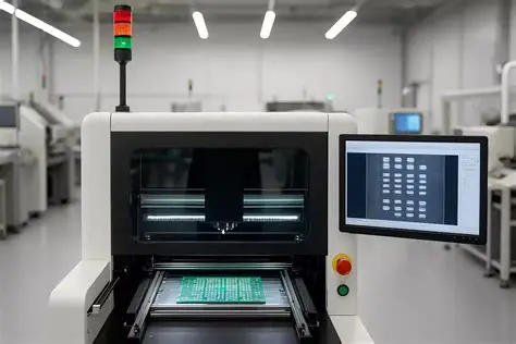
Maintaining stable environmental conditions in the printing area supports consistent results regardless of chosen stencil thickness. Temperature and humidity influence paste behavior, so controlled settings reduce variability that could mask thickness-related effects. Operators verify stencil alignment and cleanliness before each run to ensure apertures function as intended. When switching between different board designs, teams evaluate whether a single stencil thickness meets requirements or whether multiple stencils are justified.
Process capability studies help quantify how thickness choices affect defect rates. Data collected from printed boards and subsequent reflow outcomes guide refinements. Collaboration between design and manufacturing engineers ensures that stencil specifications align with both electrical performance needs and assembly constraints. This integrated approach reduces the likelihood of thickness-related issues reaching final inspection.
Related Reading: Step Stencil Thickness: How to Determine the Ideal Value for Your PCB
Conclusion
Stencil thickness remains one of the most influential parameters in achieving controlled solder paste deposition with laser cut stencils. Understanding its effect on volume supports better decisions that improve joint quality and reduce common assembly defects. Practical evaluation during process development, combined with attention to aperture design and printing parameters, delivers consistent outcomes across varied board configurations. Ongoing attention to these factors helps assembly operations maintain high reliability standards.
FAQs
Q1: How does stencil thickness affect solder volume in PCB assembly?
A1: Stencil thickness directly controls the amount of solder paste that passes through the apertures onto the board pads. Thicker stencils increase deposited volume, which suits components needing more solder for robust joints, while thinner options limit volume to prevent bridging on fine-pitch devices. Engineers evaluate this relationship during stencil design to match the specific component mix and board layout requirements.
Q2: What factors determine the optimum stencil thickness for a given PCB?
A2: Optimum stencil thickness depends on the range of component sizes, pad dimensions, and required solder joint profiles. Assembly teams consider aperture aspect ratios and the overall board complexity when making this choice. Practical testing and review of printed results help confirm that the selected thickness produces acceptable deposits across all features.
Q3: Can changing stencil thickness resolve common solder paste defects?
A3: Adjusting stencil thickness often addresses volume-related defects such as insufficient solder or excessive deposits that lead to bridging. Teams first verify that aperture design and print parameters are optimized before modifying thickness. When thickness changes prove necessary, they are implemented with corresponding checks on release efficiency and final joint quality.
Q4: Why is laser cut stencil thickness important for consistent solder paste deposition?
A4: Laser cut stencils maintain precise thickness uniformity that supports repeatable paste transfer volumes. This consistency reduces variation in deposited solder across a production batch. Manufacturers rely on this precision when targeting low defect rates and high process capability in surface mount assembly.
References
J-STD-005 - Requirements for Soldering Pastes. IPC, current revision
IPC-A-610 - Acceptability of Electronic Assemblies. IPC, current revision