 ALLPCB


Introduction
The rollout of 5G networks has introduced new frequency bands that place greater demands on printed circuit board performance. Engineers must account for both sub-6 GHz spectrum and millimeter-wave bands when developing boards for base stations, user equipment, and infrastructure. Higher operating frequencies affect signal integrity, material behavior, and overall system reliability in ways that differ from previous generations. Design teams therefore evaluate trace geometry, dielectric properties, and thermal paths early in the layout process. These considerations help maintain consistent performance across varying environmental conditions.
Why 5G Frequency Bands Matter in PCB Design
5G technology operates across two primary ranges: sub-6 GHz and mmWave frequencies above 24 GHz. Sub-6 GHz bands deliver wider coverage and better penetration through obstacles, while mmWave bands provide higher data rates but experience greater propagation losses. PCB designers must match board characteristics to the specific frequency range of the application to avoid excessive signal degradation. The choice of operating band directly influences decisions on layer stackup, copper thickness, and via placement. Understanding these differences allows teams to optimize boards for either coverage-focused or capacity-focused deployments.
Technical Principles of Frequency Impact on Signal Behavior
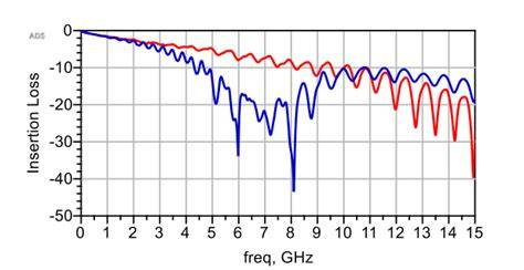
Signal attenuation rises with frequency because conductor losses increase due to the skin effect, where current concentrates near the surface of traces. Dielectric losses also grow because the loss tangent of the substrate material becomes more significant at higher frequencies. In mmWave designs, even small variations in dielectric constant can shift impedance and create reflections that degrade performance. Sub-6 GHz circuits tolerate conventional FR-4 materials more readily, yet still require tighter control of trace width and spacing to maintain signal quality. Engineers model these effects using electromagnetic simulation to predict insertion loss and return loss before fabrication.
Material Selection for 5G PCB Applications
Material selection focuses on achieving low and stable dielectric constant along with minimal loss tangent across the target frequency range. Sub-6 GHz boards often use enhanced epoxy systems that balance cost and electrical performance. mmWave designs typically require specialized laminates with lower dissipation factors to keep insertion loss within acceptable limits. Thermal expansion characteristics must also align with copper to prevent warpage during temperature cycling. IPC-6012E provides qualification requirements that help verify material suitability for high-reliability applications. Consistent material properties across production lots support repeatable electrical results.
Practical Design Practices for Sub-6 GHz and mmWave Boards
Impedance control becomes critical because even minor deviations cause reflections at 5G frequencies. Designers maintain consistent trace widths and reference plane spacing while accounting for the effect of solder mask on effective dielectric constant. Via transitions require careful back-drilling or staggered arrangements to reduce stub-induced discontinuities, especially in mmWave layouts. Ground plane integrity and stitching vias help contain electromagnetic fields and reduce crosstalk between adjacent channels. Thermal vias and copper pours distribute heat from power amplifiers and RF components to prevent localized temperature rises that could alter material properties.
Layout and Manufacturing Considerations
Routing strategies differ between frequency bands. Sub-6 GHz layouts allow somewhat longer traces, whereas mmWave circuits benefit from the shortest possible paths and minimal bends to limit radiation and loss. Panelization and handling procedures must prevent mechanical stress that could affect fine features required at higher frequencies. Surface finish selection influences high-frequency performance because certain finishes introduce additional roughness or oxidation risks. IPC-A-600K outlines acceptability criteria that guide inspection of finished boards for surface and conductor quality. Controlled impedance testing during fabrication confirms that the finished product meets the intended electrical specifications.
Conclusion
5G frequency bands require PCB designers to apply more rigorous analysis of loss mechanisms, material behavior, and layout geometry than earlier wireless standards. Sub-6 GHz and mmWave applications each present distinct challenges that influence material choice, stackup configuration, and manufacturing controls. Adherence to established industry specifications supports consistent quality and long-term reliability. By addressing these factors systematically, engineering teams can develop boards that meet the performance expectations of modern 5G systems.
FAQs
Q1: How does 5G mmWave PCB design differ from sub-6 GHz PCB design?
A1: mmWave designs demand lower-loss materials, shorter trace lengths, and more precise impedance control because signal attenuation increases rapidly above 24 GHz. Sub-6 GHz boards can often use standard materials with moderate adjustments to stackup and routing. Both approaches still require careful attention to thermal management and via transitions.
Q2: What is the typical 5G PCB frequency range that affects material selection?
A2: 5G PCB frequency range spans from below 6 GHz up to 40 GHz and beyond in mmWave bands. Material selection must account for rising dielectric losses and the skin effect as frequency increases, prompting the use of laminates with stable dielectric constants and low loss tangents.
Q3: Why is 5G PCB signal attenuation a greater concern at mmWave frequencies?
A3: 5G PCB signal attenuation grows with frequency due to conductor and dielectric losses. At mmWave frequencies, even small increases in loss tangent or surface roughness can cause unacceptable signal degradation, requiring specialized materials and layout techniques to maintain link budget.
Q4: How does 5G PCB material selection influence overall system performance?
A4: Proper 5G PCB material selection controls dielectric constant stability and loss characteristics across the operating band. Consistent material properties support predictable impedance, lower insertion loss, and reduced thermal expansion mismatch, all of which contribute to reliable high-speed signal transmission.
References
IPC-6012E — Qualification and Performance Specification for Rigid Printed Boards. IPC, 2017
IPC-A-600K — Acceptability of Printed Boards. IPC, 2020
JEDEC J-STD-020E — Moisture/Reflow Sensitivity Classification. JEDEC, 2014


