 ALLPCB


Introduction
In PCB design, creating accurate component footprints remains a critical yet time-intensive task for electrical engineers. Manual drafting of land patterns often leads to inconsistencies that affect manufacturability and reliability. Online component libraries address this by providing verified PCB footprint databases accessible via component search functions. These resources streamline the process, allowing designers to download ready-to-use footprints that align with industry standards. By integrating such tools into workflows, engineers reduce errors and accelerate project timelines. This guide explores how online libraries enhance footprint creation efficiency.
What Are Online Component Libraries?
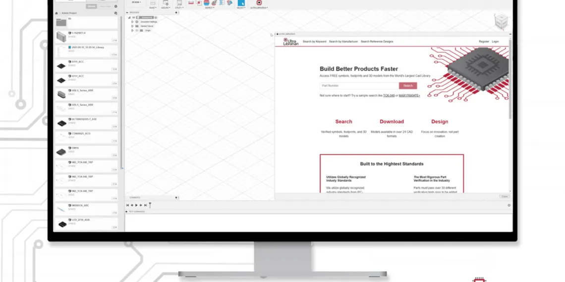
Online component libraries serve as centralized repositories hosting thousands of pre-verified footprints, symbols, and 3D models for electronic components. A PCB footprint database within these libraries contains land patterns optimized for surface-mount and through-hole devices. Engineers use component search features to locate specific parts by manufacturer, package type, or part number. Once found, footprint download options enable direct import into design software. These libraries ensure consistency across teams by standardizing formats compatible with common EDA environments. Beyond footprints, they often include parametric data for simulation and analysis.
The evolution of these platforms reflects the growing complexity of component packages in modern electronics. Engineers benefit from user-contributed validations alongside professional curation. Regular updates keep libraries current with new component releases. Effective library management involves organizing downloaded assets to avoid duplication. In essence, online component libraries transform fragmented local files into a unified, searchable ecosystem.
Why Streamlining Footprint Creation Matters
Accurate footprints directly impact solder joint integrity, assembly yields, and long-term board performance. Inaccurate land patterns can cause issues like bridging, insufficient solder volume, or mechanical stress during reflow. For electrical engineers, relying on ad-hoc creations increases design iteration cycles and risks non-compliance with fabrication tolerances. Online libraries mitigate these by offering footprints derived from standardized dimensions, reducing design time by up to 80% in high-volume projects. This efficiency scales particularly well in multi-board systems where component reuse is common.
Streamlining also fosters collaboration in distributed teams. A shared PCB footprint database ensures all members access identical data, minimizing variants. Procurement benefits too, as verified footprints correlate with supplier datasheets, easing part selection. Ultimately, these tools elevate design quality while aligning with lean engineering principles.
Technical Principles of Component Footprints
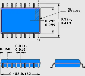
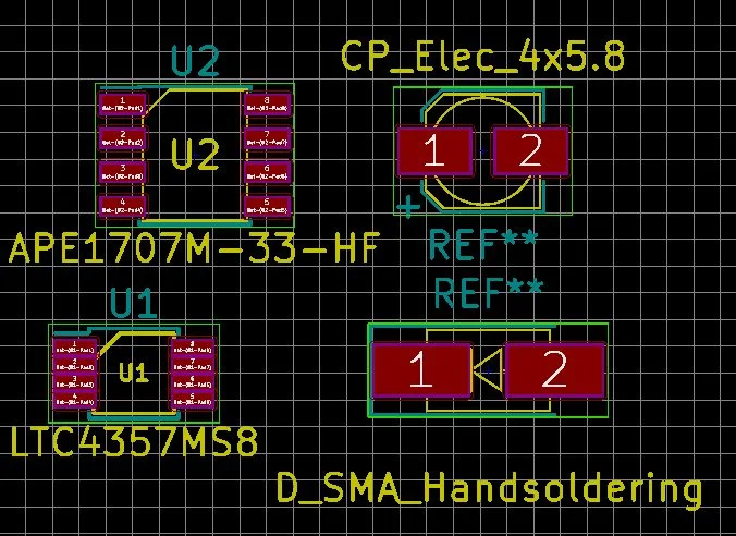
Component footprints define the copper pads, solder mask openings, and silkscreen outlines on a PCB to mate with a device's leads or balls. Design begins with the component's mechanical outline, typically sourced from datasheets, followed by pad geometry calculations. Key parameters include pad size, pitch, toe, heel, and side overhangs to optimize solder fillet formation. IPC-7351B outlines three density levels—most, nominal, and least—for balancing manufacturability and space constraints. Engineers select density based on assembly process capabilities and board density requirements.
Package body dimensions influence footprint extent, with courtyards defining minimum clearances between adjacent components. Thermal pads for QFN or BGA packages require via patterning for heat dissipation. Polarization markers and fiducials aid assembly alignment. These elements ensure electrical connectivity while accommodating tolerances in component placement accuracy, typically 50 microns for high-precision SMT.
Reflow soldering dynamics further dictate footprint shape. Solder paste volume must fill gaps without excess, preventing defects like voids or head-in-pillow. Simulations validate designs by modeling paste release and joint formation.
Leveraging Component Search in Online Libraries
Effective component search starts with precise queries using keywords like package code, pin count, or body size. Advanced filters in PCB footprint databases refine results by technology—SMT, THT—or density level. Engineers cross-reference multiple libraries for comprehensive coverage, noting format availability like IPC-7351 or ODB++. Download previews allow inspection of padstack details before commitment.
Search efficiency improves with parametric indexing, where libraries tag footprints by electrical ratings or environmental specs. For obsolete parts, variant matching suggests equivalents. Integration APIs in some systems automate pulls into design canvases. Mastering these features cuts search time from hours to minutes.
Related Reading: Mastering PCB Footprint Design: A Step by Step Guide for Beginners
Best Practices for Footprint Download and Verification
Begin footprint download by confirming datasheet alignment, especially lead coplanarity and ball shear specs. Post-download, verify against JEDEC outlines for package dimensions, ensuring no scaling errors. Import into EDA software and run design rule checks (DRC) for pad-to-pad spacing and annular ring compliance. Customize if needed, such as adding test points or adjusting for specific solder mask expansion.
Library management practices include versioning downloaded files with source metadata and date. Organize by category—resistors, ICs, connectors—in hierarchical folders. Periodic audits remove deprecated entries. For high-reliability designs, cross-validate with J-STD-001 criteria for solder joint acceptability. These steps safeguard against propagation of errors in future revisions.
Batch downloads for bill-of-materials (BOM) streamline multi-component projects. Collaborate via cloud-synced libraries for team consistency.
Challenges in Online Library Usage and Solutions
One common challenge is format incompatibilities between libraries and EDA tools. Solution: standardize on neutral formats like those from IPC-7351B and use converters. Variant proliferation for the same part across manufacturers confuses selection; mitigate with canonical naming conventions. Outdated footprints pose risks for evolving packages—address through subscription alerts or RSS feeds.
Data integrity varies; user-generated content may lack rigorous validation. Prioritize professionally curated sections and perform 3D step model overlays. Bandwidth limitations slow large downloads—opt for lightweight 2D first, then 3D. By anticipating these, engineers maximize online component library value.
Related Reading: Common PCB Footprint Errors and How to Avoid Them
Advanced Library Management Techniques
Robust library management employs database software to catalog assets with metadata tags for quick retrieval. Automate synchronization scripts to update local caches from online sources. Implement approval workflows for custom modifications. Analytics track usage patterns, highlighting frequently accessed footprints for optimization.
Integration with PLM systems links footprints to lifecycle data, aiding obsolescence management. Version control akin to Git prevents overwrite issues. These techniques scale for enterprise environments, ensuring traceability.
Conclusion
Online component libraries revolutionize PCB footprint creation by offering accessible, standardized PCB footprint databases and intuitive component search tools. Electrical engineers gain from reduced manual effort, enhanced accuracy per IPC and JEDEC guidelines, and superior library management. Adopting best practices in download, verification, and maintenance yields reliable designs ready for production. As component complexity rises, these resources remain indispensable for efficient workflows. Embrace them to elevate your PCB design process.
FAQs
Q1: What is a PCB footprint database, and how does it support component search?
A1: A PCB footprint database is a digital repository of land patterns for electronic components, enabling precise component search by parameters like package type or pin count. Engineers query for matches, preview details, and initiate footprint downloads directly into design tools. This accelerates schematic-to-layout transitions while ensuring standard compliance, reducing errors in high-density boards.
Q2: How do online component libraries improve library management?
A2: Online component libraries centralize footprints, symbols, and models, simplifying library management through search, categorization, and update mechanisms. Designers avoid redundant local files by downloading verified assets on-demand. Version tracking and metadata enhance organization, supporting team collaboration and BOM synchronization for scalable projects.
Q3: What role does footprint download play in PCB design efficiency?
A3: Footprint download from online libraries provides pre-verified land patterns, bypassing manual creation and minimizing IPC-7351 deviations. Quick imports cut design cycles, with built-in previews ensuring compatibility. Verification post-download confirms solderability, streamlining from concept to fabrication.
Q4: Can online libraries handle custom or non-standard components?
A4: Yes, many online component libraries offer tools for custom footprint generation based on user inputs, aligned with JEDEC outlines. Parametric wizards compute pads per density levels. For exotics, upload datasheets for community validation, enhancing library management without full redesign.
References
IPC-7351B — Generic Requirements for Surface Mount Design and Land Pattern Standard. IPC, 2010
JEDEC JEP95 — Registered Outlines for Solid State and Related Products. JEDEC, 2000
IPC J-STD-001H — Requirements for Soldered Electrical and Electronic Assemblies. IPC, 2017


