 ALLPCB


Introduction
Step stencils play a critical role in modern surface mount technology assembly, allowing precise control over solder paste volumes across diverse component heights on a single printed circuit board. In solder paste printing, these stencils feature varying foil thicknesses to deposit thicker paste for large components like connectors while using thinner sections for fine-pitch devices such as BGAs. However, the transition areas between thickness levels introduce challenges that demand careful management. Step stencil keep-out zones define restricted regions around these transitions where aperture placement must be avoided to ensure reliable paste release and prevent defects. Ignoring these zones during stencil design rules can lead to inconsistent printing results, compromising downstream assembly yields. This article explores the principles, design rules, and practical troubleshooting for step stencil keep-out zones, tailored for electrical engineers optimizing high-density boards.
What Are Step Stencil Keep-Out Zones and Why They Matter
Step stencils differ from uniform-thickness stencils by incorporating step-up or step-down regions, enabling a single printing pass for mixed-technology boards. A keep-out zone is the clearance area surrounding the edge of a step transition, prohibiting apertures to avoid interference during squeegee sweeping and paste release. These zones are essential in stencil design rules because solder paste behavior changes near thickness variations, potentially causing smearing or incomplete transfer. In practice, violating aperture placement guidelines near steps results in bridging between pads or insufficient paste volume, which manifests as tombstoning or open joints post-reflow. For electrical engineers, adhering to these zones directly impacts first-pass yield in high-volume production. Ultimately, proper keep-out management aligns with industry standards like IPC-7525, ensuring stencil manufacturing produces robust tools for repeatable solder paste printing.
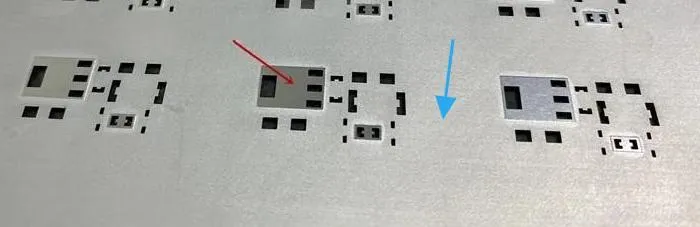
Engineers often encounter boards with components ranging from 01005 passives to large QFNs, making step stencils indispensable for volume control. Without adequate keep-out zones, the squeegee blade can scoop paste from adjacent thicker areas into thinner ones, leading to defects detectable via solder paste inspection. This issue escalates in lead-free processes where paste viscosity demands even tighter control. Keep-out zones mitigate these risks by providing buffer space for paste shear forces to stabilize. In troubleshooting scenarios, reviewing keep-out compliance reveals root causes for inconsistent printing across panels.
Technical Principles of Step Stencil Keep-Out Zones
Solder paste printing relies on the rheology of the paste, which exhibits thixotropic behavior under squeegee pressure, allowing it to flow into apertures and release cleanly upon stencil separation. In step stencils, the abrupt change in foil thickness disrupts this flow, creating shear gradients that can trap paste or cause tunneling along step walls. Keep-out zones counteract this by isolating apertures from turbulent flow regions near the step edge. Aperture placement too close to the step risks partial filling or bridging due to uneven pressure distribution across the stencil surface. Electrical engineers must consider foil tension and frame design, as these influence how the stencil flexes during printing, amplifying keep-out importance.
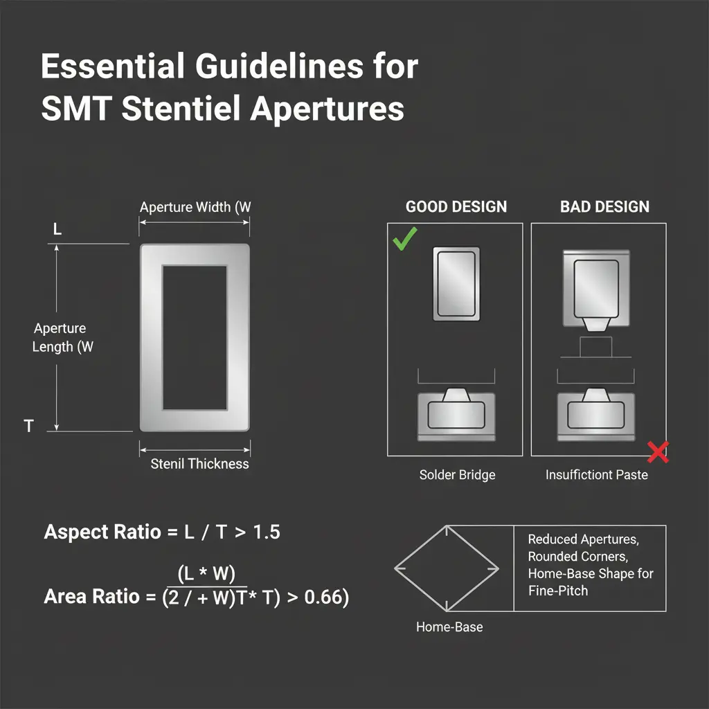
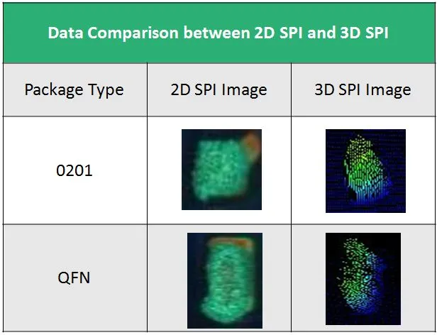
The mechanics involve the area ratio of apertures, defined as open area to wall area, which must favor release over adhesion for optimal transfer efficiency. Step transitions alter local pressure, potentially reducing this ratio near the keep-out boundary. During stencil manufacturing, laser etching precision ensures step walls are smooth, but design rules dictate zone sizing based on step height differential to accommodate manufacturing tolerances. Paste release improves when apertures align perpendicular to squeegee direction, minimizing sidewall adhesion. Violations lead to "scooping" in step-up areas or starving in step-downs, observable in volume variation data from SPI tools.
Surface energy of the stencil foil interacts with paste particles, influencing detachment. Nano-coatings on stencils enhance release but do not eliminate the need for keep-out zones, as mechanical factors dominate near steps. In high-speed printing, gSnap-off distance and speed further stress these zones, requiring conservative aperture placement. Understanding these principles guides engineers in simulating print performance before fabrication.
Related Reading: Step Stencil Thickness: How to Determine the Ideal Value for Your PCB
Design Rules for Step Stencil Keep-Out Zones
Stencil design rules for step stencil keep-out zones prioritize proportional clearances scaled to the thickness step size, as outlined in IPC-7525 guidelines. For step-down stencils, common in fine-pitch applications, the keep-out extends from the step edge into the thinner foil area, preventing apertures from encroaching where paste flow is unstable. Step-up designs, used for overprinting larger pads, require similar isolation on the thicker side to avoid excess paste migration. Aperture placement must respect these zones across the entire panel, including fiducials and borders, to maintain alignment during printing. Electrical engineers should verify rules during Gerber review, ensuring no overlaps.
General principles include orienting apertures parallel to the print direction where possible and grouping by thickness to minimize step count. In stencil manufacturing, frameless designs demand larger overall margins, amplifying keep-out impacts. Rules also address mixed printing with through-holes, where keep-out prevents paste smear into vias. Compliance reduces variability in paste height, critical for reflow profiling.
- Step-Down: Prioritize clearance in the thinner area from the step edge to isolate fine-pitch apertures from thick paste flow.
- Step-Up: Maintain clearance in the thicker area from the step edge to prevent scooping into adjacent thin zones.
- Overprint: Manage keep-outs on both sides of the step to balance volume for tall components.
Multi-level steps compound risks, necessitating cumulative keep-outs. Engineers troubleshoot by measuring zone adherence in ODB++ files.
Related Reading: Step Stencils: A Deep Dive into Multi Level Aperture Design for Complex PCB Assemblies
Best Practices and Troubleshooting for Optimal Printing
Implement best practices by starting with IPC-7525-compliant templates for aperture reduction, typically scaling to pad size while honoring keep-outs. Select stencil thickness based on the smallest pitch, stepping up only where necessary to limit transitions. During solder paste printing trials, monitor transfer efficiency near zones using SPI, adjusting squeegee pressure if variability exceeds 10 percent. Troubleshoot bridging by increasing keep-out or refining step geometry; starving often traces to insufficient zone width or paste rheology mismatch.
Validate stencil manufacturing via profilometer checks on step heights and wall angles. For persistent issues, consider hybrid stencils but prioritize single-step designs for simplicity. Post-print cleaning cycles help, but design rules prevent root causes.
In production, panelize with shared keep-outs across arrays to optimize material. Regular audits ensure stencil design rules evolve with component trends.
Common Troubleshooting Scenarios
Engineers frequently face inconsistent paste volumes near steps, signaling keep-out violations. Inspect Gerbers for aperture proximity, then prototype with relaxed zones if space-constrained. Bridging in step-down areas responds to aperture elongation or window-paneing. For step-up overprint failures, verify squeegee hardness matches foil tension.
Document trials to refine rules per paste type.
Conclusion
Mastering step stencil keep-out zones elevates solder paste printing reliability, directly boosting assembly yields for complex boards. By integrating stencil design rules into aperture placement, engineers mitigate flow disruptions at transitions. Adhering to guidelines like those in IPC-7525 ensures stencil manufacturing yields durable tools. Practical troubleshooting reinforces these principles, turning potential defects into predictable processes. Prioritize zone clearances early in design for optimal results across production runs.
FAQs
Q1: What is a step stencil keep-out zone in solder paste printing?
A1: A step stencil keep-out zone is a restricted area around thickness transitions where no apertures are placed to prevent paste flow issues. This ensures clean release and uniform deposition during printing. Proper sizing per stencil design rules avoids bridging or insufficient volume near fine-pitch components. Electrical engineers use it to handle mixed-height boards reliably.
Q2: How do stencil design rules define aperture placement near keep-out zones?
A2: Stencil design rules specify clearances proportional to step height differences, isolating apertures from turbulent areas. Aperture placement must avoid the zone to maintain paste shear stability. Violations cause defects like smearing, addressed by Gerber checks. IPC-7525 provides foundational guidelines for consistent application.
Q3: Why are step stencil keep-out zones critical in stencil manufacturing?
A3: During stencil manufacturing, keep-out zones accommodate laser precision and foil stress, preventing print inconsistencies. They scale with step depth to counter mechanical interferences. Ignoring them leads to yield losses in high-density assembly. Troubleshooting focuses on zone verification for optimal performance.
Q4: What common defects arise from poor step stencil keep-out zone management?
A4: Poor management causes bridging, paste starvation, or uneven heights near steps, impacting reflow. Symptoms include tombstoning or voids, traced via SPI. Remedies involve enlarging zones or refining aperture shapes. Adhering to design rules minimizes these in production.
References
IPC-7525B — Stencil Design Guidelines. IPC, 2011
IPC-7525C — Stencil Design Guidelines. IPC, 2011


