 ALLPCB


In the fast-evolving world of electronics, printed circuit boards (PCBs) are the backbone of countless devices, from consumer gadgets to industrial systems. For high-density and high-performance designs, stacked vias have become a critical feature. But how reliable are stacked vias under demanding conditions? Stacked via reliability is essential to ensure robust performance in challenging PCB applications. In this comprehensive guide, we'll explore stacked via reliability testing, PCB thermal cycling, via cracking risks, material selection for stacked vias, PCB failure analysis, and strategies for improving PCB durability. Whether you're an engineer or a designer, this blog will provide actionable insights to help you build stronger, more dependable PCBs.
What Are Stacked Vias and Why Do They Matter?
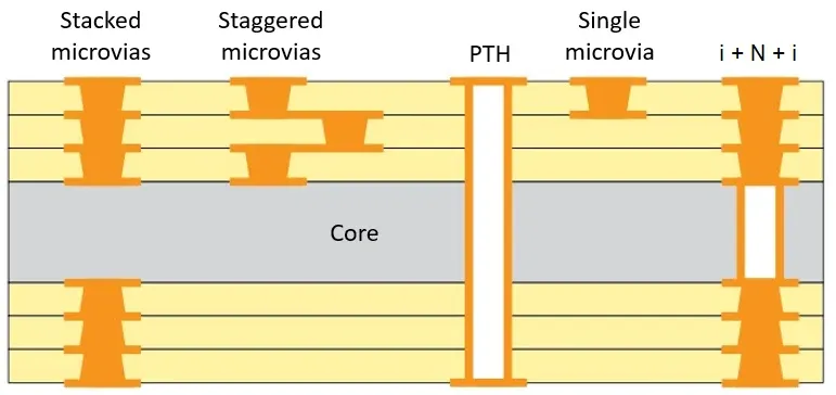
Stacked vias are a type of vertical interconnect used in multilayer PCBs to connect different layers directly on top of each other, rather than staggering them. This design saves space and enables high-density interconnects (HDI), which are crucial for modern electronics like smartphones, medical devices, and aerospace systems. However, their compact nature can introduce reliability challenges, especially under thermal stress or mechanical strain.
The reliability of stacked vias directly impacts the overall performance of a PCB. A failure in a single via can lead to signal loss, power interruptions, or complete system breakdowns. Understanding how to design and test stacked vias for durability is vital for applications where failure is not an option.
Key Challenges in Stacked Via Reliability
Stacked vias face several challenges that can compromise their performance. Let’s break down the most common issues:
1. Thermal Stress from PCB Thermal Cycling
PCBs often operate in environments with significant temperature fluctuations. During PCB thermal cycling, materials expand and contract at different rates due to their unique coefficients of thermal expansion (CTE). For stacked vias, this can create stress at the via walls and surrounding copper layers, potentially leading to cracks or delamination. Studies suggest that thermal cycling between -55°C and 125°C, a common range for testing, can cause micro-cracks in vias after just a few hundred cycles if not designed properly.
2. Via Cracking and Mechanical Stress
Via cracking is a frequent failure mode in stacked vias, often caused by mechanical stress during manufacturing or operation. For instance, drilling misalignments or excessive pressure during assembly can weaken the via structure. Cracks may start small but can grow under repeated stress, leading to open circuits. Data from reliability tests shows that via cracking can reduce the lifespan of a PCB by up to 30% in high-stress environments.
3. Material Mismatch and Fatigue
The materials used in and around stacked vias play a big role in their durability. A mismatch in CTE between the via fill material, copper plating, and the PCB substrate can lead to fatigue over time. This is especially true for applications with frequent power cycles or high operating temperatures, where material fatigue can cause failures after as few as 1,000 thermal cycles.
Stacked Via Reliability Testing: Methods and Standards
To ensure stacked vias can withstand demanding conditions, rigorous testing is necessary. Stacked via reliability testing simulates real-world stresses to identify potential weaknesses before they cause failures. Here are the key testing methods:
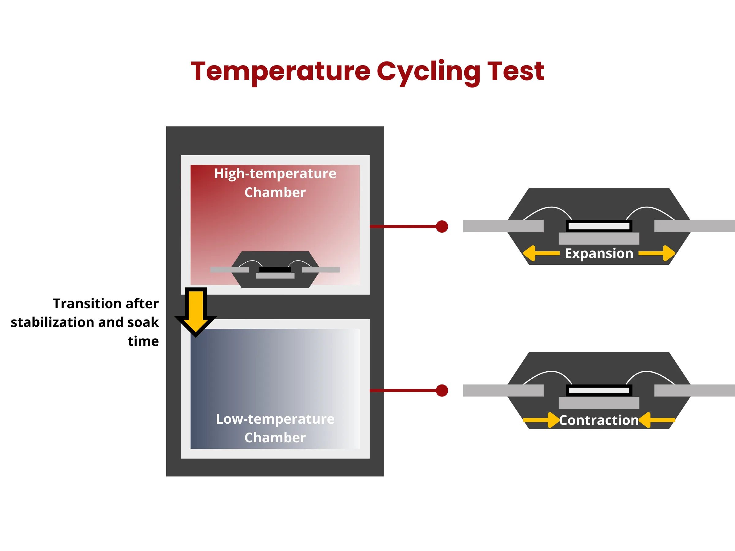
Thermal Cycling Tests
Thermal cycling tests expose PCBs to alternating high and low temperatures to mimic operational conditions. A typical test might cycle between -40°C and 85°C for 1,000 cycles, monitoring for changes in electrical resistance or structural integrity. According to industry standards like IPC-TM-650, a resistance increase of more than 10% in a via indicates a potential reliability issue.
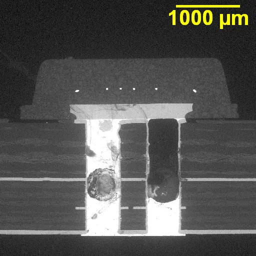
Microsection Analysis
After thermal cycling, microsection analysis is often used to visually inspect stacked vias for cracks or delamination. This involves cutting a cross-section of the PCB and examining it under a microscope. This method helps engineers detect issues like incomplete via filling or poor copper plating adhesion, which can compromise reliability.
Highly Accelerated Life Testing (HALT)
HALT pushes PCBs beyond their normal operating limits to uncover design flaws. For stacked vias, HALT might combine extreme temperatures (e.g., -55°C to 150°C) with vibration stress to simulate harsh environments like those in automotive or aerospace applications. This aggressive testing can reduce the time to failure from months to days, helping designers address issues early.
Material Selection for Stacked Vias: Building a Strong Foundation
Choosing the right materials is a critical step in improving stacked via reliability. Here are some key considerations for material selection for stacked vias:
Via Fill Materials
Stacked vias are often filled with conductive or non-conductive materials to enhance strength and conductivity. Epoxy-based conductive fills are popular for their balance of cost and performance, offering good thermal conductivity (around 1-3 W/m·K) and resistance to cracking. For high-reliability applications, copper-filled vias provide superior conductivity (up to 400 W/m·K) but are more expensive and harder to process.
Substrate Materials
The PCB substrate must have a CTE close to that of the via materials to minimize stress during thermal cycling. FR-4, a common substrate, has a CTE of about 14-17 ppm/°C, which works well for many applications. However, for high-performance designs, materials like polyimide (CTE around 12-14 ppm/°C) or high-Tg FR-4 (CTE around 10-12 ppm/°C) offer better thermal stability.
Copper Plating Quality
The copper plating in stacked vias must be uniform and free of voids to ensure reliable electrical connections. Poor plating can lead to high resistance or cracking under stress. Industry standards recommend a minimum copper thickness of 25 micrometers for via walls in HDI designs to withstand thermal and mechanical loads.
PCB Failure Analysis: Identifying and Addressing Via Issues
When stacked vias fail, PCB failure analysis helps uncover the root cause and prevent future issues. Here are the steps typically involved:
1. Electrical Testing
Electrical testing measures continuity and resistance across vias to detect open or short circuits. A via with resistance exceeding 10 milliohms after thermal cycling may indicate a crack or poor connection.
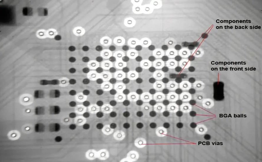
2. Visual and X-Ray Inspection
Non-destructive X-ray inspection can reveal internal defects like voids or misalignments in stacked vias without damaging the PCB. Visual inspection under magnification can also identify surface cracks or delamination at via pads.
3. Root Cause Analysis
Once a failure is detected, engineers analyze factors like design flaws, manufacturing defects, or material mismatches. For example, a via crack might stem from excessive drill depth during manufacturing, which can be corrected by adjusting process parameters.
Strategies for Improving PCB Durability with Stacked Vias
Improving PCB durability starts with optimizing the design and manufacturing of stacked vias. Here are practical strategies to enhance reliability:
Optimize Via Design
Design stacked vias with aspect ratios (depth-to-diameter) below 1:1 to reduce stress during drilling and plating. For instance, a via with a 0.2 mm diameter should not exceed 0.2 mm in depth per layer. Additionally, avoid placing vias too close to board edges or mounting holes, where mechanical stress is higher.
Use Simulation Tools
Thermal and mechanical simulation tools can predict how stacked vias will behave under stress. For example, finite element analysis (FEA) can model CTE mismatches and identify high-stress areas, allowing designers to adjust layouts before production. Simulations have been shown to reduce design iterations by up to 40% in complex HDI projects.
Implement Robust Manufacturing Processes
Ensure precise drilling and plating during manufacturing to avoid defects like over-etching or incomplete fills. Using laser drilling for microvias in stacked structures can achieve tighter tolerances (down to 0.1 mm) compared to mechanical drilling, improving reliability.
Adopt Industry Standards
Follow standards like IPC-6012 for PCB fabrication and IPC-TM-650 for testing to ensure consistent quality. These guidelines specify acceptable limits for via resistance, copper thickness, and thermal stress performance, helping to build durable designs.
Real-World Applications of Reliable Stacked Vias
Stacked vias are critical in industries where reliability is non-negotiable. In aerospace, PCBs with stacked vias must endure extreme thermal cycling (e.g., -55°C to 125°C) and vibration without failure. In automotive electronics, they support high-density connections in control units, operating reliably for over 10 years under harsh conditions. Medical devices, such as pacemakers, also rely on stacked vias for compact, dependable designs that cannot afford to fail.
By focusing on reliability testing and material selection, engineers can ensure stacked vias meet the stringent demands of these applications. For instance, a well-designed stacked via in an automotive PCB can maintain signal integrity at speeds up to 10 Gbps, even after 2,000 thermal cycles.
Conclusion: Building Better PCBs with Reliable Stacked Vias
Stacked vias are a cornerstone of high-density PCB designs, but their reliability is paramount for demanding applications. By understanding the challenges of PCB thermal cycling, addressing via cracking risks, and making informed decisions on material selection for stacked vias, engineers can significantly improve PCB durability. Through rigorous stacked via reliability testing and thorough PCB failure analysis, potential issues can be identified and resolved before they impact performance.
At ALLPCB, we’re committed to helping you achieve robust, high-performance PCB designs. By applying the strategies outlined in this guide—optimizing via design, selecting the right materials, and adhering to industry standards—you can ensure your PCBs stand up to the toughest conditions. Whether you're working on consumer electronics or critical systems, reliable stacked vias are the key to long-lasting, dependable performance.


