 ALLPCB


Introduction
Telecommunication base stations depend on specialized printed circuit boards to handle signal processing, power distribution, and data transmission under demanding conditions. Effective base station PCB maintenance helps minimize service interruptions and supports network reliability across large coverage areas. Engineers routinely address issues through structured PCB troubleshooting and targeted PCB repair procedures. These activities form a core part of sustaining long-term performance in outdoor and high-traffic installations. Proper planning and adherence to established methods reduce the likelihood of recurring faults.
Why Base Station PCB Maintenance Matters
Base station PCBs operate continuously in environments that include wide temperature swings, humidity, vibration, and electromagnetic interference. Neglecting maintenance can lead to progressive degradation that affects signal integrity and overall system uptime. Regular PCB failure analysis allows teams to identify early signs of wear before they escalate into full outages. Organizations that implement consistent base station PCB maintenance programs typically experience fewer emergency interventions and lower operational costs over time. This proactive approach aligns with the need for dependable infrastructure in modern telecommunications networks.
Common Causes of Failures in Base Station PCBs
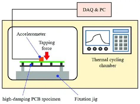
Environmental stresses represent a primary driver of issues in these assemblies. Thermal cycling causes repeated expansion and contraction that fatigues solder joints and component leads over extended periods. Moisture ingress promotes corrosion on exposed conductors and can create conductive paths that trigger short circuits. Vibration from wind, equipment movement, or seismic activity loosens mechanical connections and accelerates crack propagation in laminates. Manufacturing variations, such as inconsistent plating thickness or voids in vias, may also contribute when combined with field conditions. Electrical surges from lightning or power fluctuations further stress sensitive semiconductors and passive components.
PCB Failure Analysis Techniques
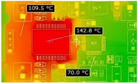
Systematic PCB failure analysis begins with non-destructive visual and microscopic inspection to locate obvious defects such as lifted pads, cracked traces, or discoloration from overheating. Engineers then apply thermal imaging to detect hot spots that indicate excessive current draw or poor thermal dissipation. Electrical testing with multimeters, oscilloscopes, and boundary scan tools helps isolate open circuits, shorts, and intermittent faults without immediate disassembly. When required, destructive methods like cross-sectioning or delayering reveal internal issues such as delamination or via barrel cracking. Documentation of each step supports root cause determination and guides subsequent corrective actions.
PCB Rework and Repair Best Practices
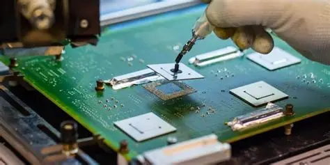
Successful PCB rework requires controlled environments and calibrated equipment to avoid introducing new damage during component removal or replacement. Technicians follow temperature profiles that respect the thermal mass of the board and nearby parts to prevent warpage or delamination. Flux selection and solder alloy compatibility ensure reliable new joints while minimizing residue that could affect long-term insulation resistance. Trace and pad repairs often involve conductive epoxy or jumper wires applied according to precise layout guidelines. Post-repair cleaning removes flux residues, and conformal coating restoration protects against future environmental exposure. Throughout the process, adherence to IPC-7711/7721 procedures provides consistent methodology for achieving acceptable results.
Industry standards such as J-STD-001 complement these efforts by defining acceptable soldering criteria that apply equally to original assembly and subsequent repair operations. Verification after rework includes electrical continuity checks, insulation resistance measurements, and visual inspection against established acceptance criteria. Training programs that emphasize these protocols help maintain skill levels across maintenance teams. Scheduling preventive inspections at regular intervals further supports early detection of wear patterns specific to base station installations.
Troubleshooting Workflow for Field Engineers
A practical troubleshooting sequence starts with reviewing system logs and performance data to narrow the suspected board or subsystem. On-site visual checks for physical damage or contamination precede more detailed bench testing when the assembly can be safely removed. Isolation of power and signal paths helps confirm whether the fault lies in passive networks, active devices, or interconnects. When multiple boards exhibit similar symptoms, pattern analysis often points to shared environmental or design factors. Iterative testing and minimal intervention preserve evidence for deeper analysis if initial repairs do not fully resolve the issue.
Conclusion
Reliable operation of telecommunication base stations depends on disciplined base station PCB maintenance combined with methodical PCB troubleshooting and PCB repair practices. Understanding failure mechanisms enables targeted interventions that restore functionality without compromising long-term durability. Following established industry procedures ensures consistency and repeatability across different sites and teams. Continued emphasis on training and documentation strengthens overall network resilience. These measures collectively contribute to sustained service quality in demanding field conditions.
FAQs
Q1: What are the most frequent triggers for PCB repair in base station environments?
A1: Environmental factors such as thermal cycling, moisture, and vibration commonly initiate degradation that requires PCB repair. Regular monitoring through PCB failure analysis helps detect these issues early and guides timely intervention.
Q2: How does PCB troubleshooting differ for base station assemblies compared with indoor equipment?
A2: Base station PCB troubleshooting must account for outdoor exposure effects including corrosion and mechanical stress in addition to standard electrical diagnostics. Field conditions often necessitate portable test equipment and non-destructive methods before any board removal.
Q3: What role does PCB rework play in extending the service life of telecommunication hardware?
A3: Targeted PCB rework restores functionality to boards affected by component failure or localized damage, avoiding full replacement in many cases. When performed according to recognized procedures, it maintains original performance margins while addressing specific defects.
Q4: Why is systematic PCB failure analysis important before attempting repairs?
A4: Systematic PCB failure analysis identifies root causes rather than symptoms, preventing repeated failures after repair. It also informs whether rework, replacement, or design adjustments represent the most effective long-term solution.
References
IPC-7711/7721C — Rework, Modification, and Repair of Electronic Assemblies. IPC, 2017
J-STD-001J — Requirements for Soldered Electrical and Electronic Assemblies. IPC, 2024
IPC-A-610H — Acceptability of Electronic Assemblies. IPC, 2020





