 ALLPCB


Power Integrity and Signal Integrity: A Symbiotic Relationship
Power integrity and signal integrity represent two fundamental aspects of high-speed PCB design that directly influence each other. Engineers must address both simultaneously to achieve reliable system performance. Power rail fluctuations can degrade signal quality, while noisy signals can increase current demands on the power distribution network. This interaction becomes especially critical in designs operating at higher frequencies or with dense component placement. Understanding their relationship helps designers create boards that meet performance targets without excessive iteration.
What Power Integrity and Signal Integrity Mean in PCB Design
Power integrity focuses on delivering stable voltage to all active devices across the printed circuit board. It involves managing the power delivery network, or PDN, to minimize voltage drops and noise. Signal integrity ensures that transmitted signals maintain their intended shape and timing from driver to receiver. Poor power integrity often manifests as power rail noise that couples into signal paths. Conversely, simultaneous switching noise generated by multiple outputs changing state at once can stress the PDN. These effects create a feedback loop that designers must break through careful planning.
Industry standards such as IPC-2221B provide guidance on printed board design practices that support both power and signal requirements. The symbiotic nature means that optimizing one domain frequently improves the other when layout decisions consider both from the start.
Technical Principles Behind Their Interaction
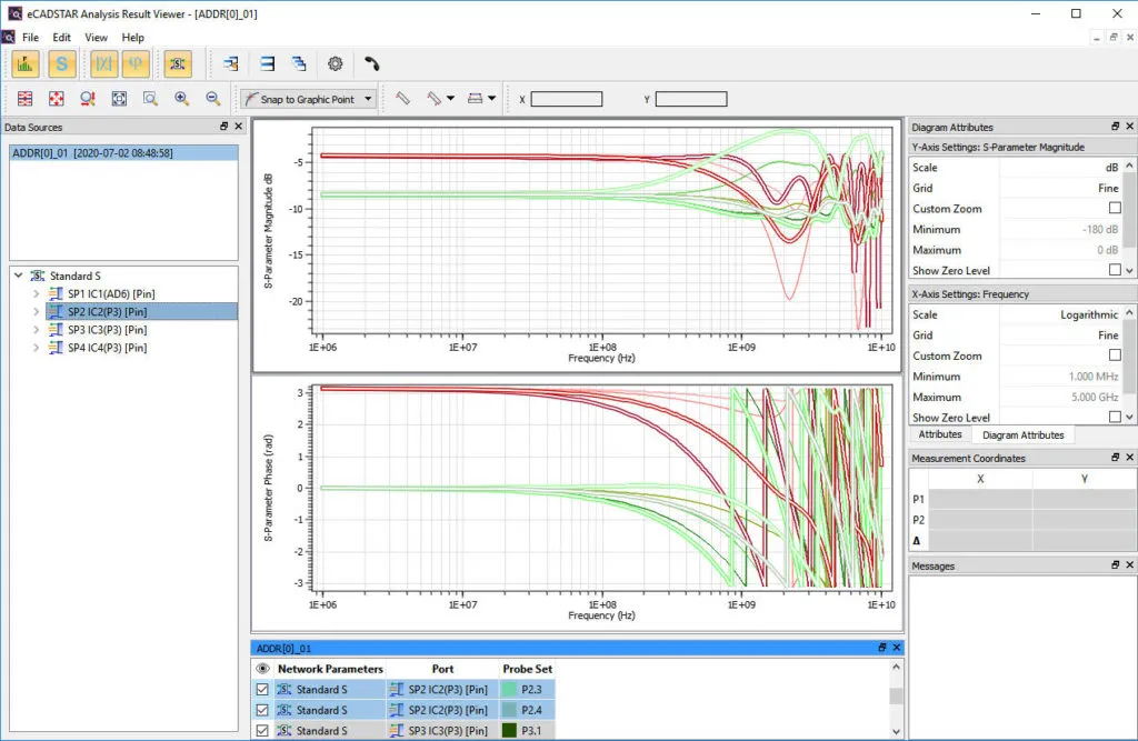
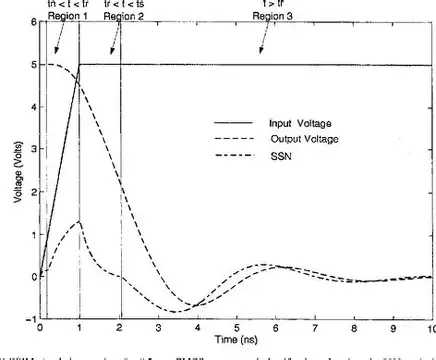
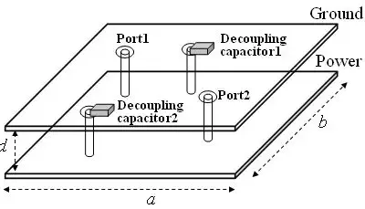
The PDN consists of planes, traces, vias, and decoupling components that supply current to integrated circuits. Inductance in this network causes voltage variations when current demand changes rapidly. Power rail noise arises from these variations and can appear as ripple or spikes that modulate reference voltages used by signal circuits. Simultaneous switching noise occurs when many outputs switch together, drawing large transient currents that the PDN must supply instantly. This noise can propagate through shared return paths and affect nearby signals.
Signal integrity suffers when power noise alters driver output levels or receiver thresholds. Ground bounce and power bounce further complicate the picture by shifting reference potentials. The interaction intensifies at higher data rates because signal edges become faster and more sensitive to supply variations. Proper stackup planning and return path continuity reduce unwanted coupling between power and signal domains.
Practical Solutions and Best Practices for Engineers
Designers begin by defining target impedance for the PDN across the frequency range of interest. Decoupling capacitors placed close to device power pins lower impedance at higher frequencies. Plane capacitance between power and ground layers provides low-impedance paths at mid frequencies. Via placement and stitching ensure low-inductance connections between layers. Signal routing avoids crossing splits in reference planes to maintain continuous return paths.
Power and signal layout decisions should occur together rather than sequentially. Placing sensitive signals away from high-current power paths reduces coupling. Controlled impedance routing combined with proper termination minimizes reflections that could otherwise increase power consumption. Simulation of both domains early in the process reveals interactions before fabrication. Post-layout extraction and analysis confirm that power rail noise remains within acceptable limits for the chosen signaling scheme.
Industry standards such as IPC-6012E outline qualification requirements that indirectly support robust power and signal performance through material and construction specifications. Following these guidelines helps ensure the fabricated board meets the intended electrical characteristics.
Conclusion
Power integrity and signal integrity function as interdependent elements in modern PCB design. Addressing power rail noise and simultaneous switching noise requires attention to the full power delivery network and its influence on signal paths. Structured layout practices, appropriate decoupling strategies, and adherence to relevant standards reduce unwanted interactions. Engineers who treat the two domains as a single system achieve more predictable results and fewer design revisions.
FAQs
Q1: How does power integrity affect signal integrity in high-speed designs?
A1: Power rail noise from an inadequate PDN can shift voltage references and introduce jitter or amplitude distortion into signals. This interaction becomes pronounced during simultaneous switching events that create transient current demands. Proper PDN design with sufficient decoupling helps maintain clean signal transmission.
Q2: What role does simultaneous switching noise play in power integrity signal integrity interaction?
A2: Simultaneous switching noise generates voltage droops on power rails that can corrupt signal levels and timing. The resulting noise couples through shared ground or power paths into adjacent signal lines. Managing this requires coordinated placement of decoupling components and careful return path design.
Q3: Why is PDN design critical when addressing both power integrity and signal integrity?
A3: A well-designed PDN keeps voltage stable across operating conditions, preventing power noise from degrading signal quality. Low-impedance paths at relevant frequencies reduce the impact of current transients on both power rails and signal references. This stability supports reliable operation at higher speeds.
Q4: What layout practices help minimize power integrity signal integrity problems?
A4: Placing decoupling capacitors near device pins, maintaining continuous reference planes, and avoiding plane splits under signal routes reduce coupling. Coordinated stackup planning and via optimization further limit inductance in both power and return paths. These steps address the symbiotic relationship directly during layout.
References
IPC-2221B — Generic Standard on Printed Board Design. IPC, 2012
IPC-6012E — Qualification and Performance Specification for Rigid Printed Boards. IPC, 2017
JEDEC J-STD-020E — Moisture/Reflow Sensitivity Classification. JEDEC, 2014


