ALLPCB


Introduction
High-Density Interconnect (HDI) PCBs represent the pinnacle of modern printed circuit board technology, enabling compact designs with superior performance in applications like smartphones, medical devices, and aerospace systems. These boards feature microvias, fine pitch components, and high-density assembly that push the limits of traditional inspection methods. Optical inspection alone falls short because many critical features, such as internal via plating and hidden solder joints, remain invisible from the surface. X-ray inspection emerges as an indispensable tool for HDI PCBs, providing non-destructive visibility into these obscured areas to ensure reliability and functionality. Factory production lines increasingly integrate X-ray for HDI to meet stringent quality requirements, reducing field failures and rework costs. This article explores the technical necessity of X-ray for HDI, detailing its principles, applications, and best practices aligned with industry standards.
Understanding HDI PCBs and the Critical Role of X-ray Inspection
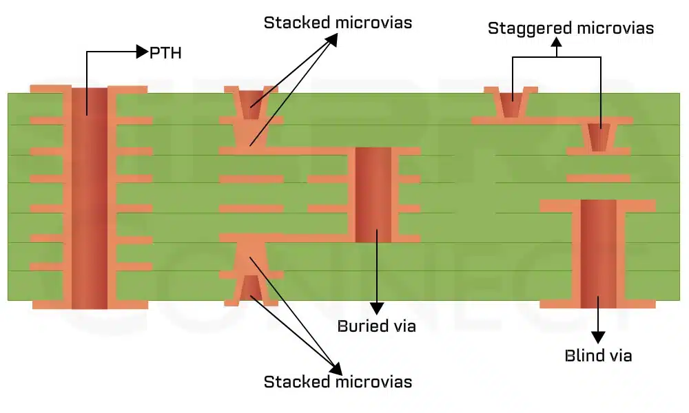
HDI PCBs incorporate advanced features like laser-drilled microvias with diameters under 150 microns, stacked and staggered via configurations, and trace widths as narrow as 30 microns to achieve higher wiring density than conventional boards. Fine pitch components, often with pitches below 0.4 mm, and high-density assembly demand precise placement and interconnection that challenge visual verification. Traditional automated optical inspection (AOI) excels at surface defects but cannot penetrate multi-layer structures to assess via fill quality or subsurface solder fillet formation. X-ray for HDI addresses this gap by transmitting radiation through the board to generate images of internal structures, revealing defects like voids, cracks, or incomplete fills that compromise electrical performance. In high-volume manufacturing, undetected issues in microvias or ball grid array (BGA) joints lead to intermittent failures under thermal stress or vibration. Adopting X-ray inspection ensures compliance with qualification criteria for HDI PCBs, safeguarding product integrity from prototype to production.
The escalating complexity of HDI designs amplifies the risks associated with hidden defects. Microvias, essential for interlayer connections, require uniform copper plating to prevent resistance hotspots or delamination during reflow. Fine pitch components increase the likelihood of bridging or insufficient solder volume, which optical methods overlook. High-density assembly further complicates matters, as component shadows obscure underlying features. X-ray systems differentiate materials by density, highlighting discrepancies in solder joints or via metallurgy. This capability proves vital for electric engineers optimizing layouts for signal integrity while maintaining manufacturability.
Technical Principles of X-ray Inspection in HDI PCB Manufacturing
X-ray inspection operates on the principle of differential absorption, where X-rays penetrate the PCB and are attenuated by denser materials like copper or solder more than by dielectrics or air. Detectors capture the transmitted rays to form grayscale images, with high-density features appearing darker. For HDI PCBs, 2D real-time X-ray provides rapid scanning suitable for inline production, tilting the board to view under components for fine pitch analysis. However, 3D computed tomography (CT) offers superior resolution by reconstructing volumetric data from multiple angles, essential for stacked microvias where planar views mislead. Resolution down to 1 micron enables detection of plating thickness variations or void percentages exceeding acceptable limits. Factory engineers calibrate systems for optimal kV and μA settings based on board thickness, typically 50-150 kV for HDI stacks.
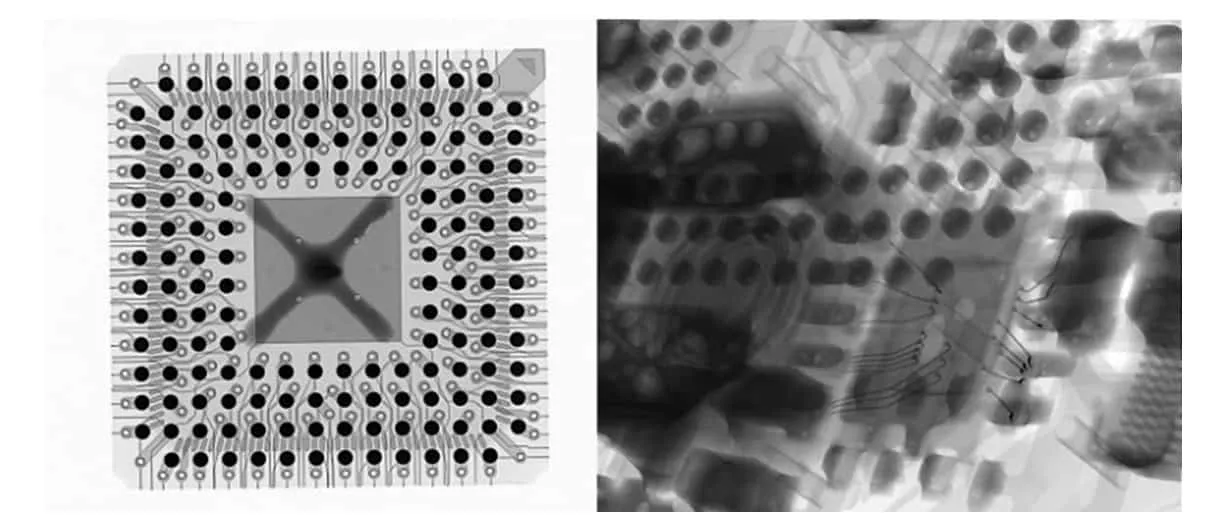
In microvia inspection, X-ray verifies fill completeness, distinguishing between electroplated copper, conductive paste, or resin plugs. Per IPC-2226 guidelines for HDI design, microvias must maintain aspect ratios below 1:1 to ensure reliable plating, but X-ray confirms post-process integrity by measuring barrel wall uniformity. Defects like keyholing, where plating thins at the via bottom, manifest as density gradients. For fine pitch components, X-ray reveals tombstoning or skewing indirectly through joint fillet shadows. High-density assembly benefits from oblique-angle imaging to inspect BGAs, identifying head-in-pillow effects where the solder ball fails to fully wet the pad.
Solder joint analysis dominates X-ray for HDI applications, focusing on voids, bridges, and fillet shapes under opaque packages. Voids larger than 25% of joint area indicate reflow issues, while insufficient solder volume signals paste printing errors. X-ray distinguishes open joints from full wets by contrast differences. Multi-layer HDI boards challenge penetration, requiring higher energy for deeper layers without overexposing surface features. Automated X-ray systems employ image processing algorithms for defect classification, correlating grayscale thresholds to acceptance criteria. This precision aligns with IPC-A-610 requirements for electronic assemblies, ensuring class 3 products meet high-reliability standards.
Best Practices for X-ray Inspection in HDI PCB Production
Integrate X-ray inspection early in the HDI manufacturing workflow, post-lamination for bare board microvia checks and post-reflow for assembled boards. Inline placement after SMT ovens catches defects before downstream processes, minimizing scrap rates. Select system resolution matching feature sizes, with sub-5 micron spot size for microvias under 75 microns. Calibrate daily using reference standards to maintain grayscale accuracy across operators. Combine X-ray with AOI for hybrid inspection, leveraging optical for topside and X-ray for subsurface, optimizing throughput in high-density assembly lines.
Optimize imaging parameters for HDI specifics: lower kV for thin stacks to enhance contrast in fine pitch areas, higher flux for thicker builds. Program automated tilt sequences to capture multiple joint views, reducing operator dependency. Train personnel on artifact recognition, such as beam hardening in high-copper regions, to avoid false calls. Document inspection zones prioritizing critical nets, like power delivery vias prone to voiding. Per IPC-6016 performance specifications for HDI boards, establish defect thresholds tied to reliability testing, ensuring process capability indices exceed 1.33.
For high-volume runs, implement statistical process control with X-ray data, tracking void populations or via fill metrics over shifts. Feedback loops adjust stencil apertures or reflow profiles based on trends in fine pitch joint quality. Validate new HDI designs with cross-section correlations to baseline X-ray interpretations. This factory-driven approach sustains yield improvements while adhering to quality management principles.
Troubleshooting Defects in HDI PCBs Using X-ray Inspection
Electric engineers frequently encounter microvia voids in HDI PCBs, appearing as dark elliptical regions on X-ray images due to trapped air during plating. Root causes include excessive aspect ratios or inadequate desmear, resolvable by refining laser parameters and etch chemistry. Stacked microvias show interlayer misalignment as offset shadows, prompting via capture pad enlargement per design rules. Fine pitch QFN components reveal non-wet opens as uniform low-density zones, traced to paste volume deficiencies fixed via stencil thickness adjustments.
BGA head-in-pillow defects, common in high-density assembly, display as rounded ball-pad separations on tilted X-rays. Thermal profile mismatches cause this, mitigated by ramp-soak-peak optimizations. Bridging in fine pitch arrays appears as extraneous high-density links, signaling aperture crosstalk corrected by laser-cut stencils. Post-analysis, section affected boards to confirm X-ray findings, correlating with electrical tests. Systematic logging builds a defect library, accelerating root cause analysis in future lots.
Conclusion
X-ray inspection stands as a cornerstone for HDI PCB quality control, uniquely equipped to verify microvias, fine pitch components, and high-density assembly features invisible to other methods. By revealing voids, plating issues, and joint anomalies, it upholds reliability in demanding applications. Factory implementation of best practices, from inline integration to parameter tuning, maximizes its value while aligning with standards like IPC-2226 and IPC-A-610. Engineers benefit from data-driven troubleshooting, enhancing design-manufacturing synergy. Prioritizing X-ray for HDI ensures robust products, reduced failures, and competitive edge in electronics innovation.
FAQs
Q1: What defects does X-ray inspection detect in HDI PCBs that AOI misses?
A1: X-ray for HDI penetrates layers to identify microvia voids, BGA solder joint cracks, and via plating inconsistencies, which AOI cannot see beneath surfaces. Fine pitch components hide bridges or insufficient fillets from optical views. Factory data shows X-ray catches over 80% more subsurface issues, aligning with IPC-A-610 criteria for high-reliability assemblies. This non-destructive method supports high-density assembly without halting production.
Q2: How does X-ray verify microvia quality in HDI PCBs?
A2: X-ray images display density variations in microvia fills, confirming uniform copper plating or paste distribution per IPC-6016 specifications. Voids or keyholing appear as low-density spots, guiding process tweaks like aspect ratio control. Tilted 3D CT enhances accuracy for stacked configurations. Engineers use grayscale thresholds to quantify fill percentages, ensuring electrical continuity in compact designs.
Q3: When should X-ray be used in high-density assembly for fine pitch components?
A3: Apply X-ray post-reflow for fine pitch BGA and QFN joints to check wetting and voids invisible externally. Inline after SMT for real-time feedback on high-density assembly. Combine with electrical testing for comprehensive validation. This practice prevents escapes in HDI PCBs, maintaining yield in volume production.
Q4: Is 2D or 3D X-ray better for HDI PCB inspection?
A4: 2D X-ray suits high-speed inline checks for fine pitch overviews, while 3D CT excels at volumetric analysis of microvias and complex joints. Choose based on defect risk: 2D for routine, 3D for qualification. Both support HDI standards, with 3D resolving overlaps in dense stacks for precise troubleshooting.
References
IPC-2226 — Design Standard for High Density Interconnect (HDI). IPC, 2001 (revised)
IPC-A-610H — Acceptability of Electronic Assemblies. IPC, 2019
IPC-6016D — Qualification and Performance Specification for High Density Interconnect (HDI) Printed Boards. IPC, 2013