 ALLPCB


Introduction
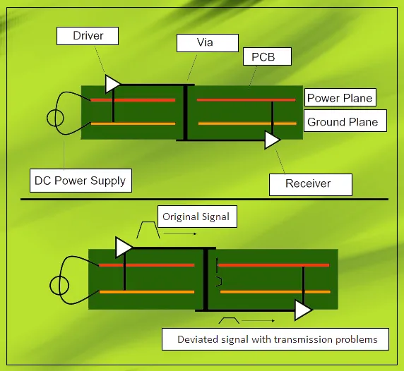
Signal integrity challenges dominate high-speed PCB designs, where even minor routing flaws can compromise system performance. Electrical engineers face issues like trace stubs, plane voids, and ground plane breaks that introduce reflections, crosstalk, and impedance discontinuities. These defects disrupt signal propagation, leading to timing errors, bit flips, and outright failures in data-intensive applications. Identifying them early during the design and fabrication stages saves costly respins and ensures compliance with performance demands. This article delves into the mechanisms behind these problems, their impacts on signal integrity, and structured approaches to detection and mitigation. By mastering PCB routing techniques, engineers can build robust boards that maintain clean waveforms across frequencies.
In modern electronics, operating speeds exceeding gigahertz amplify the sensitivity to these issues. Trace stubs arise from unnecessary via extensions, plane voids from fabrication gaps in copper pours, and ground plane breaks from splits or cuts under signal lines. Each contributes uniquely to signal distortion, yet they share common roots in layout decisions and manufacturing tolerances. Understanding their signatures through simulation and inspection tools empowers proactive fixes. Ground planes serve as critical return paths, so any interruption elevates inductance and noise coupling.
The Fundamentals of Signal Integrity in PCBs
Signal integrity refers to the preservation of electrical signal quality from transmitter to receiver, encompassing amplitude, rise time, and timing fidelity. In PCB routing, it hinges on controlled impedance, minimal reflections, and low crosstalk between adjacent traces. Disruptions occur when transmission line principles falter, such as mismatched characteristic impedance or unintended stubs acting as antennas. Engineers must consider dielectric properties, trace geometry, and reference plane continuity to sustain integrity. High-speed signals demand microstrip or stripline configurations with solid adjacent planes for return currents.
Why does signal integrity matter in today's PCBs? Rising edge rates in protocols like PCIe, DDR, and Ethernet shorten wavelengths, making board dimensions comparable to signal periods. A stub just millimeters long can resonate at GHz frequencies, causing severe ringing. Plane voids increase loop inductance, elevating EMI susceptibility. Ground plane breaks force return currents to detour, amplifying ground bounce and crosstalk. Neglecting these leads to marginal eye diagrams, reduced margins, and field failures. Proactive design per established guidelines prevents such pitfalls.
Trace Stubs: Causes and Effects on Signal Propagation
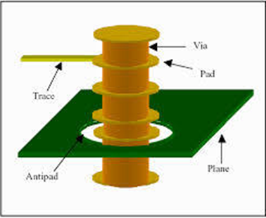
Trace stubs emerge primarily from vias where unused portions extend beyond the signal path, creating open-ended discontinuities. In multilayer boards, blind or buried vias minimize stubs, but through-hole vias often leave tails on inner layers. These stubs reflect signals due to impedance mismatch at the open end, with reflection coefficient approaching 1 for high frequencies. The effect intensifies as stub length nears a quarter-wavelength of the signal frequency, turning it into a bandpass filter that attenuates harmonics. Engineers observe this as overshoot, undershoot, or eye closure in time-domain reflectometry (TDR) measurements.
Fabrication tolerances exacerbate stub issues if drill depths vary or back-drilling fails. In high-density interconnects, fanout from BGA packages multiplies via counts, heightening stub risks without proper staggering. Signal integrity simulations reveal stub-induced jitter, degrading bit error rates. To quantify, a 1 mm stub at 5 GHz introduces significant phase shift, demanding mitigation. Regular design reviews catch these during routing, prioritizing stubless topologies.
IPC-2221C outlines generic requirements for conductor routing and via placement, emphasizing minimization of discontinuities for reliable performance. Adhering to its principles guides stub avoidance in complex layouts.
Plane Voids: Impacts on Impedance and Return Paths
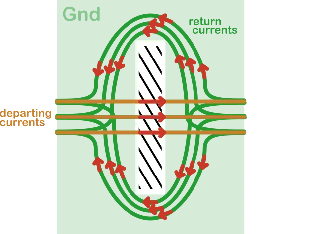
Plane voids are gaps or missing copper in power or ground planes, often from etching non-uniformities, photoresist adhesion failures, or design splits. Under a signal trace, these voids sever the low-inductance return path, forcing currents to spread laterally across the plane. This elevates effective inductance, slows rise times, and boosts crosstalk to neighboring traces. In stripline configurations, voids directly alter characteristic impedance, causing mismatches observable in TDR as impedance dips. High-current planes suffer thermal hotspots around voids, compounding electromigration risks over time.
Detection relies on automated optical inspection (AOI) or cross-section analysis during fabrication qualification. Voids larger than trace width significantly degrade signal integrity, especially in dense routing where return paths compete. Engineers mitigate by oversizing pours and verifying fill in Gerber reviews. In multilayer stackups, aligning voids away from critical nets preserves integrity.
Manufacturing processes influence void formation, with plating chemistry and panel size playing roles. Consistent electrolyte control reduces defects, ensuring plane integrity aligns with performance specs.
Ground Plane Breaks: The Silent Killer of Reference Integrity
Ground plane breaks, or splits, occur from routing channels cut through solid pours, component clearances, or intentional power islands. Signals crossing these breaks experience return path lengthening, as currents detour around the void, increasing loop area and inductance. This manifests as increased insertion loss, ground bounce during switching, and enhanced EMI radiation. In differential pairs, asymmetric breaks unbalance common-mode rejection, skewing eye patterns. Frequency-domain analysis shows peaks at break resonances, confirming the issue.
Design intent often causes breaks, like isolating analog grounds, but poor execution amplifies problems. Vias stitching across splits help, but wide channels demand multiple rows. IPC-A-600M defines acceptability criteria for plane conductor continuity, flagging excessive breaks as defects in visual inspections. Compliance ensures boards meet class 3 requirements for high-reliability apps.
Breaks near connectors or ICs worsen simultaneous switching noise (SSN), coupling into power rails. Layer sequencing with dedicated ground planes adjacent to signals minimizes exposure.
Best Practices for Robust PCB Routing and Signal Integrity
Effective PCB routing starts with stackup planning, placing high-speed signals between full ground planes for tight coupling. Maintain 3:1 trace-to-plane spacing ratios to contain fields. Use length-matched routing for clocks and data buses, avoiding 90-degree bends that introduce stubs. Back-drill vias longer than half the board thickness to stub lengths below 10 mils. IPC-6012F specifies qualification tests verifying plane performance and conductor integrity post-fabrication.
Incorporate guard traces or shielding for sensitive nets, grounded via-fenced to planes. Simulate pre-layout with field solvers to predict TDR and S-parameters. During routing, enforce DRCs for minimum anti-pad sizes preventing via-induced voids. Stagger vias in dense areas to distribute anti-pads, preserving plane solidity.
Post-route verification includes TDR scans and flying probe tests. Collaborate with fabricators on DFM feedback, adjusting clearances for etch factors. These practices yield 20-30% better margins in eye diagrams.
For plane continuity, employ stitching vias every lambda/20 along edges and splits. Differential routing benefits from symmetric reference planes, reducing skew.
Troubleshooting Signal Integrity Failures
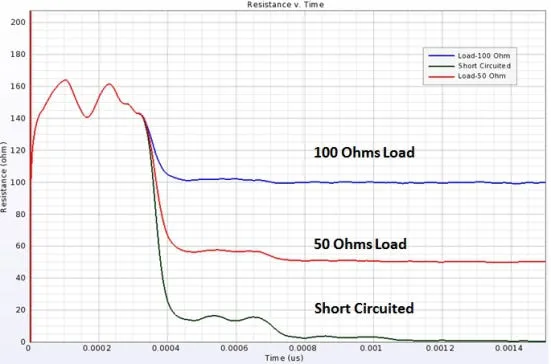
Diagnosis begins with scope captures at suspect points, hunting ringing or jitter. TDR pinpoints impedance steps from stubs or voids. X-ray or microsectioning reveals plane defects invisible to AOI. EMI chamber tests correlate radiation to ground breaks.
Isolate by de-populating suspect areas or adding test points. Simulation correlation refines models, predicting fixes like back-drilling. Iterative prototyping with quick-turn boards accelerates resolution.
Field returns often trace to overlooked routing over splits. Systematic checklists prevent recurrence.
Conclusion
Mastering signal integrity demands vigilance against trace stubs, plane voids, and ground plane breaks in PCB routing. These issues undermine high-speed performance through reflections and inductance hikes, but structured design and verification counter them effectively. Leveraging standards like IPC-2221C, IPC-A-600M, and IPC-6012F ensures compliance and reliability. Electrical engineers achieve cleaner signals by prioritizing reference planes, minimizing discontinuities, and thorough inspections. Implementing these insights optimizes board yields and system margins for demanding applications.
FAQs
Q1: What are trace stubs and how do they affect signal integrity in PCB routing?
A1: Trace stubs are unused extensions of vias or traces acting as open stubs, causing signal reflections at high frequencies. They degrade signal integrity by introducing impedance mismatches, leading to overshoot, ringing, and eye closure. Mitigation involves back-drilling or blind vias to keep stubs shorter than a twentieth of the wavelength. Simulations predict impacts early in design.
Q2: How do plane voids impact ground plane performance?
A2: Plane voids disrupt low-inductance return paths under traces, increasing loop inductance and crosstalk. In signal integrity contexts, they cause impedance variations and EMI. Inspect via AOI and cross-sections, ensuring copper fill exceeds 90% in pours. Proper plating processes minimize voids during fabrication.
Q3: Why are ground plane breaks problematic for high-speed PCBs?
A3: Ground plane breaks force return currents to detour, elevating inductance and ground bounce. They compromise signal integrity by amplifying noise coupling across splits. Avoid routing over breaks and use stitching vias. Standards guide acceptable continuity for class 3 boards.
Q4: What PCB routing best practices enhance signal integrity?
A4: Prioritize adjacent ground planes, controlled impedance traces, and stubless vias. Enforce 3W spacing to curb crosstalk, and verify with TDR. Stackup design with symmetric planes sustains performance.
References
IPC-2221C — Generic Standard on Printed Board Design. IPC, 2023
IPC-A-600M — Acceptability of Printed Boards. IPC, 2025
IPC-6012F — Qualification and Performance Specification for Rigid Printed Boards. IPC, 2023





