ALLPCB


Introduction
PCB X-ray inspection stands as a cornerstone in modern electronics manufacturing, enabling the detection of internal defects that optical methods cannot reveal. This non-destructive technique penetrates board materials to visualize solder joints, vias, and component placements, ensuring higher reliability in assemblies. For electric engineers focused on quality control, mastering X-ray best practices translates directly to reduced rework, improved yields, and compliance with rigorous standards. By optimizing inspection techniques, teams can uncover hidden issues like voids and misalignments early in the process. This article explores practical strategies to maximize the value of PCB X-ray inspection, from setup to analysis.
What Is PCB X-ray Inspection and Why It Matters
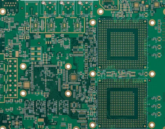
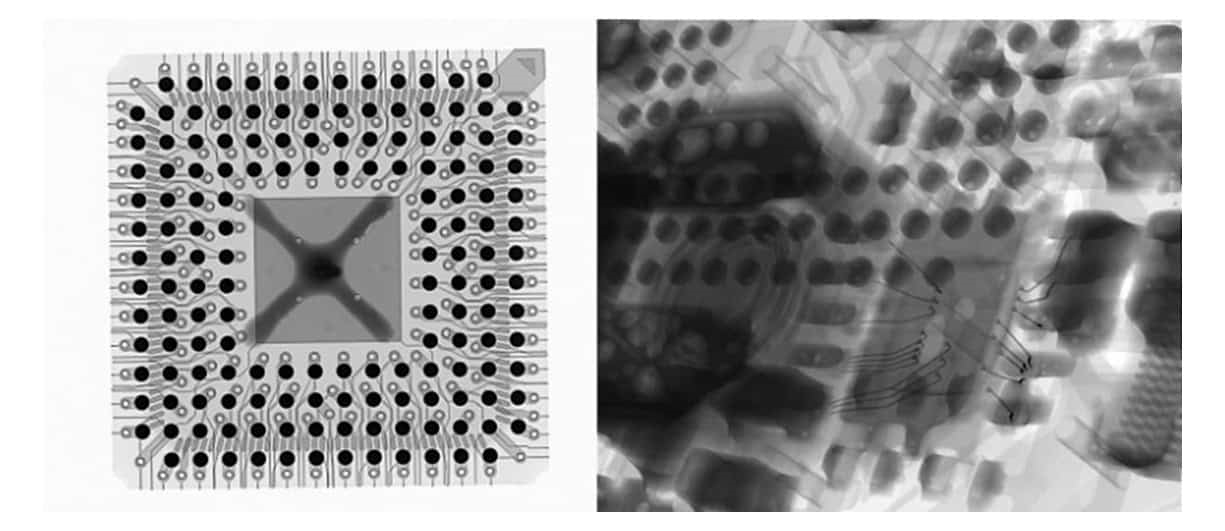
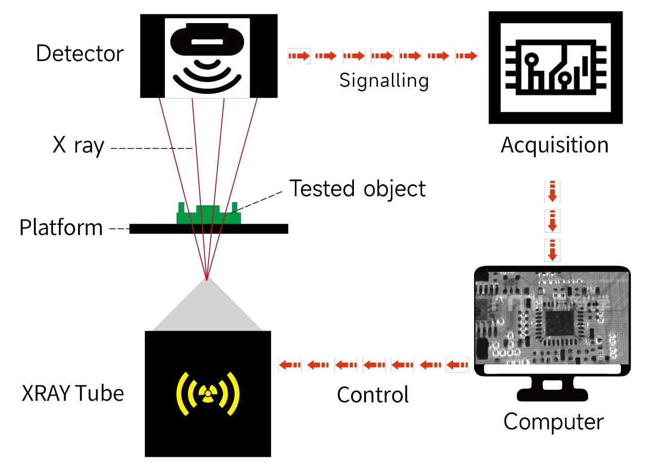
PCB X-ray inspection employs low-energy X-rays to generate transmission images of printed circuit boards, highlighting differences in material density and atomic number. Dense elements like solder appear bright against darker substrates such as FR-4, allowing visibility into hidden features. Unlike automated optical inspection, which is limited to surfaces, X-ray reveals subsurface structures in components like BGAs, QFNs, and through-hole joints. This capability proves essential for high-density assemblies where failures can lead to field returns or safety risks.
The relevance grows with shrinking component sizes and complex multilayer designs, where traditional methods fall short. Industries demanding high reliability, such as aerospace and medical, rely on it to verify solder quality and barrel fill in plated-through holes. Implementing effective inspection techniques supports process improvement by providing data for reflow profile adjustments and stencil optimizations. Ultimately, it aligns production with standards like IPC J-STD-001, which guides X-ray use for certain joint evaluations.
Technical Principles of PCB X-ray Inspection
X-ray inspection operates on the principle of differential absorption, where photons pass through materials at rates determined by thickness and composition. Heavier atoms attenuate more rays, creating contrast in the resulting image: solder joints show as bright areas, while voids appear darker. Systems typically use transmission imaging, with 2D projections for speed or 3D computed tomography for depth-resolved views. In 2D mode, a single-angle shadow map suffices for many checks, but overlapping features demand oblique angles to resolve ambiguities.
Resolution depends on focal spot size, detector pixel pitch, and magnification, enabling detection down to fine features in dense boards. Voltage and current settings influence penetration: lower for thin boards to maintain contrast, higher for multilayers to avoid underexposure. Safety features like lead shielding and interlocks ensure operator protection during operation. These principles underpin reliable defect analysis tips, allowing engineers to distinguish true anomalies from imaging artifacts.
3D techniques reconstruct volumetric data from multiple projections, isolating layers for precise void mapping in thermal pads or vias. This method excels in failure analysis but suits lower throughput compared to inline 2D systems. Understanding these mechanisms helps in selecting parameters that enhance image optimization without compromising speed.
Best Practices for Effective X-ray Inspection
Equipment Setup and Calibration
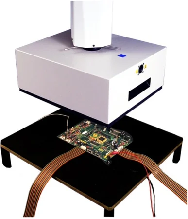
Proper equipment setup forms the foundation of X-ray best practices. Begin by verifying system calibration daily, checking alignment between source, sample, and detector to prevent distortion. Secure the PCB flat on the stage to eliminate motion blur during exposure. Adjust voltage and current iteratively based on board thickness, starting with test images on known good samples. Regular maintenance, such as filament checks and filter cleaning, sustains consistent performance.
Incorporate shielding and follow radiation safety protocols to protect personnel. For automated systems, program fiducials or CAD overlays for targeted scanning of critical areas like BGAs. These steps ensure repeatable results aligned with factory quality goals.
Sample Preparation and Inspection Techniques
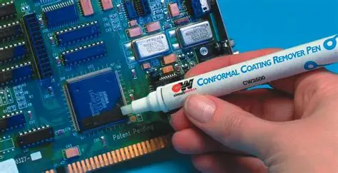
Prepare samples by removing static shielding and grounding handlers per ESD guidelines. Inspect high-risk areas first, such as bottom-side BGAs or double-sided assemblies. Employ multi-angle views, including oblique tilts up to 45 degrees, to reveal shadowed joints. Combine with other methods like AOI for comprehensive coverage: optical for surfaces, X-ray for internals.
Use inline setups for 100% inspection of key components to catch trends early. Vary scan paths for complex boards to minimize overlap artifacts. These inspection techniques boost detection rates while maintaining throughput.
Image Optimization Strategies
Image optimization starts with exposure balancing to avoid noise or saturation. Enhance contrast post-capture using software filters, edge enhancement, and grayscale inversion for voids. Zoom capabilities aid in magnifying subtle features without losing detail. Save raw data alongside processed images for verification.
For noisy images, apply averaging from multiple frames. Train operators to recognize density patterns: uniform solder darkens consistently, disruptions signal issues. These defect analysis tips refine interpretation accuracy.
Defect Analysis Tips
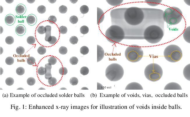
Focus analysis on common defects like voids, bridges, opens, and misalignments. Voids manifest as lighter regions within solder masses, compromising reliability. Bridges appear as unintended connections, shorts risking failures. Measure joint fill and alignment against reference images.
Cross-reference findings with IPC-A-610 criteria for acceptability, categorizing by class. Document locations with coordinates and severity for traceability. Use heatmaps for void distribution to spot process drifts. Consistent application of these tips elevates quality control.
Process Improvement Through X-ray Inspection
X-ray data drives process improvement by quantifying defect trends over batches. High void rates may indicate reflow issues, prompting profile tweaks for better wetting. Misalignments suggest stencil or placement adjustments. Statistical tracking via control charts identifies excursions early.
Feedback loops integrate findings into upstream steps, like paste printing verification. For high-volume lines, automate reporting to correlate with yield metrics. Compliance with IPC J-STD-001 ensures standardized evaluation, fostering continuous refinement. This closed-loop approach minimizes escapes and optimizes costs.
Troubleshooting Common Challenges
Blurry images often stem from vibration or misalignment; counter with stage stabilization and recalibration. Low contrast in thick boards requires voltage increases, tested incrementally. Operator variability decreases through training on standards like IPC-A-610. For overlapping features, switch to 3D or angled views.
False positives from artifacts demand good-sample comparisons. Integrate AI aids cautiously, validating against manual checks. These resolutions sustain inspection efficacy.
Conclusion
Maximizing PCB X-ray inspection benefits hinges on disciplined X-ray best practices, from calibrated setups to thorough defect analysis. Engineers gain actionable insights into hidden flaws, driving process improvement and standard compliance. Techniques like multi-angle imaging and contrast optimization unlock fuller potential, reducing risks in complex assemblies. Prioritizing these steps yields reliable products and efficient operations.
FAQs
Q1: What are key X-ray best practices for inspecting BGA components?
A1: Position the board for oblique views to access hidden joints, calibrate voltage for penetration, and optimize contrast to highlight voids or bridges. Reference IPC J-STD-001 for through-hole guidance and combine with fiducial alignment for precision. This ensures comprehensive coverage in high-density areas, supporting process improvement.
Q2: How does image optimization improve defect analysis tips in PCB X-ray inspection?
A2: Adjust grayscale and filters to differentiate densities, reducing noise for clearer void and misalignment detection. Multi-frame averaging sharpens details, while software tools quantify anomalies. These steps enhance accuracy, aligning with factory-driven quality control.
Q3: What role does PCB X-ray inspection play in process improvement?
A3: It provides defect data for reflow and stencil refinements, tracking trends to prevent recurrences. Inline integration catches issues early, boosting yields. Consistent application per standards like IPC-A-610 minimizes variability.
Q4: When should electric engineers use 3D X-ray over 2D techniques?
A4: Opt for 3D in multilayer or failure analysis for layer isolation, despite slower speed. 2D suits high-volume inline checks. Select based on complexity to balance detail and throughput.
References
IPC J-STD-001J — Requirements for Soldered Electrical and Electronic Assemblies. IPC, 2024
IPC-A-610J — Acceptability of Electronic Assemblies. IPC, 2024
IPC-6012F — Qualification and Performance Specification for Rigid Printed Boards. IPC, 2023