 ALLPCB


Introduction
Fine-pitch components such as 0.4 mm pitch BGAs and QFNs present unique demands during surface-mount assembly. Solder paste printing becomes the critical first step where stencil design directly influences deposit volume, shape, and consistency. Engineers often encounter issues like insufficient paste release, bridging between pads, and uneven height when standard stencils are applied without adjustment. These challenges arise because the reduced pad dimensions and tighter spacing leave little margin for error in paste transfer. Effective stencil design for 0.4 mm pitch BGA and stencil design for QFN therefore requires deliberate choices in aperture geometry, thickness, and surface finish to maintain process capability.
Why Stencil Design Matters for Fine-Pitch SMT
Stencil design for fine-pitch components determines how much solder paste reaches each pad and how cleanly it releases during printing. In high-density boards, even small deviations in paste volume can cause opens after reflow or create shorts that require rework. The process window narrows further when components have thermal pads or multiple rows of terminals, because paste must flow evenly across all features in a single pass. Manufacturers address these constraints by tailoring aperture size and shape to the specific pad layout rather than relying on generic rules. When stencil design for 0.4 mm pitch BGA and stencil design for QFN are executed correctly, first-pass yield improves and downstream inspection shows fewer defects.
Technical Principles Behind Fine-Pitch Solder Paste Printing Challenges
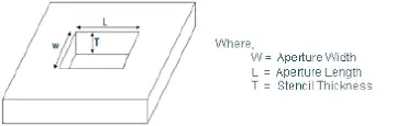
Solder paste printing challenges at fine pitch stem from the interaction between stencil aperture walls, paste rheology, and pad surface tension. As aperture width decreases, the surface area of the stencil wall relative to the opening increases, raising the risk that paste will adhere to the walls instead of transferring to the board. Area ratio and aspect ratio calculations guide aperture sizing so that the opening remains large enough for reliable release while still fitting within the pad boundaries. Stencil thickness for fine-pitch also plays a direct role; thicker foils can supply more paste volume but make release more difficult on small features. IPC-7525 outlines the fundamental relationships between these parameters and expected transfer efficiency.
Related Reading: Optimizing SMT Stencil Design for Fine Pitch Components: A Comprehensive Guide
Practical Solutions and Best Practices
Engineers begin by selecting stencil thickness for fine-pitch based on the smallest feature on the board, typically stepping down from standard thicknesses when 0.4 mm pitch BGAs or QFNs are present. Aperture design then follows with rounded or home-plate shapes that reduce the amount of stencil wall in contact with the paste. Laser-cut stainless-steel stencils with electropolished or nickel-plated surfaces further improve release by smoothing the aperture walls. During printing, squeegee pressure, speed, and separation distance are adjusted in small increments while monitoring paste height on test coupons. These steps collectively reduce bridging and insufficient deposits without requiring changes to the board layout.
Related Reading: Precision Solder Paste Application: Mastering Laser Cut Stencils for Fine-Pitch PCBs
Troubleshooting Common Fine-Pitch Issues
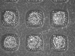
When bridging appears between adjacent pads on a 0.4 mm pitch BGA, the first check is whether aperture width exceeds the recommended percentage of pad width. Reducing aperture size by 10 to 15 percent while maintaining area ratio often resolves the problem. Insufficient paste on QFN thermal pads usually indicates that the large central aperture is not releasing paste evenly; adding a cross-hatch or segmented pattern inside the aperture improves flow. If paste volume varies across the board, warpage measurement during printing setup reveals whether the substrate is lifting at the corners.
Case Study Insight from Assembly Line Experience
One assembly team faced repeated opens on a 0.4 mm pitch BGA after switching to a thinner board laminate. Initial prints showed acceptable volume on test pads, yet functional testing revealed cold joints. Investigation traced the issue to slight board warpage that reduced contact pressure at the stencil interface. Adjusting the support tooling and adding a slight step-down in stencil thickness for fine-pitch restored consistent transfer. The change also eliminated bridging on nearby QFN components without altering the aperture design. This experience reinforced that stencil design for 0.4 mm pitch BGA must account for both component pitch and board mechanical behavior.
Conclusion
Stencil design for fine-pitch components succeeds when aperture geometry, thickness, and printing parameters are chosen together rather than in isolation. Addressing solder paste printing challenges early prevents costly defects later in the process. Practical adjustments grounded in area ratio principles and surface-finish improvements deliver repeatable results across 0.4 mm pitch BGA and QFN layouts. Continuous monitoring of deposit quality remains essential as board designs continue to increase density.
FAQs
Q1: What factors determine stencil thickness for fine-pitch components?
A1: Stencil thickness for fine-pitch is chosen according to the smallest pad width and the required paste volume. Thinner foils improve release on 0.4 mm pitch BGA and QFN pads while still supplying enough solder for reliable joints. Engineers verify the choice through test prints before committing to production panels.
Q2: How does stencil design for 0.4 mm pitch BGA differ from standard designs?
A2: Stencil design for 0.4 mm pitch BGA uses reduced aperture width and modified shapes to maintain area ratio within acceptable limits. This prevents bridging between closely spaced pads and ensures adequate paste on each ball site. The same principles apply when stencil design for QFN thermal pads is required on the same board.
Q3: What are the main solder paste printing challenges at fine pitch?
A3: Solder paste printing challenges at fine pitch include poor release from small apertures, bridging between pads, and inconsistent volume across thermal pads. These issues arise because the stencil wall area becomes large relative to the opening. Targeted aperture modifications and controlled printing parameters reduce the frequency of these defects.
Q4: Which industry standard guides fine-pitch stencil aperture design?
A4: J-STD-005 provides requirements for solder paste that influence how aperture design supports consistent deposits. Combined with IPC-7525 guidance on stencil geometry, these documents help engineers establish repeatable processes for fine-pitch stencil aperture design without relying on trial-and-error alone.
References
IPC-7525B — Stencil Design Guidelines. IPC, 2012
J-STD-005A — Requirements for Soldering Pastes. IPC, 2014
IPC-7095D — Design and Assembly Process Implementation for BGAs. IPC, 2015


