ALLPCB


Introduction
As printed circuit boards shrink to fit into compact devices like wearables, IoT sensors, and portable electronics, designing an effective power distribution network becomes increasingly complex. Smaller PCB sizes concentrate components and signals, amplifying challenges in maintaining stable power delivery. Electrical engineers must address PDN impedance in small PCBs to prevent noise, voltage fluctuations, and signal integrity issues that can degrade performance. Power plane design for compact boards requires careful planning to ensure low resistance paths and uniform current distribution. This article explores best practices for PDN design tailored to custom PCB sizes, emphasizing decoupling capacitor placement, minimizing voltage drop, and power integrity simulation. By following structured engineering approaches, designers can achieve reliable power integrity even in constrained layouts.
Understanding PDN Fundamentals and Relevance to Small PCBs
A power distribution network in a PCB consists of power and ground planes, traces, vias, and decoupling capacitors that deliver stable voltage to active components. In larger boards, PDN paths offer more flexibility for routing, but compact designs demand precise control to avoid resonances and inductive effects at high frequencies. PDN impedance in small PCBs typically needs to stay below targeted levels to support fast-switching ICs, where even minor variations cause ripple. Engineers evaluate PDN performance through target impedance curves, balancing DC resistance with AC decoupling. The relevance intensifies in high-speed applications, as smaller sizes reduce loop inductances but increase coupling between power and signal lines. Adhering to IPC-2221B guidelines ensures systematic design for power integrity across board sizes.
Power planes form the backbone of PDN, providing low-impedance return paths essential for compact boards. Ground planes shield signals and stabilize reference potentials, while splits must be managed to prevent impedance discontinuities. In small PCBs, layer count limitations force trade-offs between signal routing and dedicated power layers. Effective PDN design minimizes simultaneous switching noise, preserving margins for eye diagrams and jitter budgets. Engineers prioritize uniform current spreading to avoid hotspots that could warp boards under thermal stress.
Technical Principles of PDN Impedance in Small PCBs
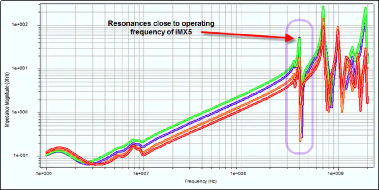
PDN impedance arises from resistive, inductive, and capacitive elements interacting across the board. In small PCBs, shorter distances lower DC resistance but heighten vulnerability to plane resonances around clock frequencies. Target impedance, calculated as Vdd / (I * ripple tolerance), guides design; for example, GHz-range switching demands sub-10 milliohm targets at key harmonics. Decoupling capacitors bridge low-frequency plane capacitance with high-frequency bypassing, forming a multi-stage filter. Vias introduce inductance, so placement density matters in compact areas. Power integrity simulation reveals these interactions via S-parameters and time-domain responses.
Inductance dominates at higher frequencies, where plane spreading inductance scales inversely with area. Small PCBs exhibit higher partial inductance per via due to reduced spreading, necessitating via farms for low-impedance paths. Capacitive coupling between planes sets the baseline impedance floor, influenced by dielectric thickness and material. Engineers model PDN as a transmission line network to predict voltage droop during transients. Fabricating prototypes without simulation risks iterations, as impedance mismatches manifest as EMI or functional failures.
Voltage drop compounds impedance issues, stemming from IR losses in conductors. Thinner traces or planes in compact designs exacerbate this, especially under peak currents. Plane resistance depends on copper weight and fill factor, while vias add contact resistance. Thermal expansion affects long-term stability, per IPC-6012E performance specs. Monitoring these ensures compliance with power budget constraints.
Best Practices for Power Plane Design for Compact Boards
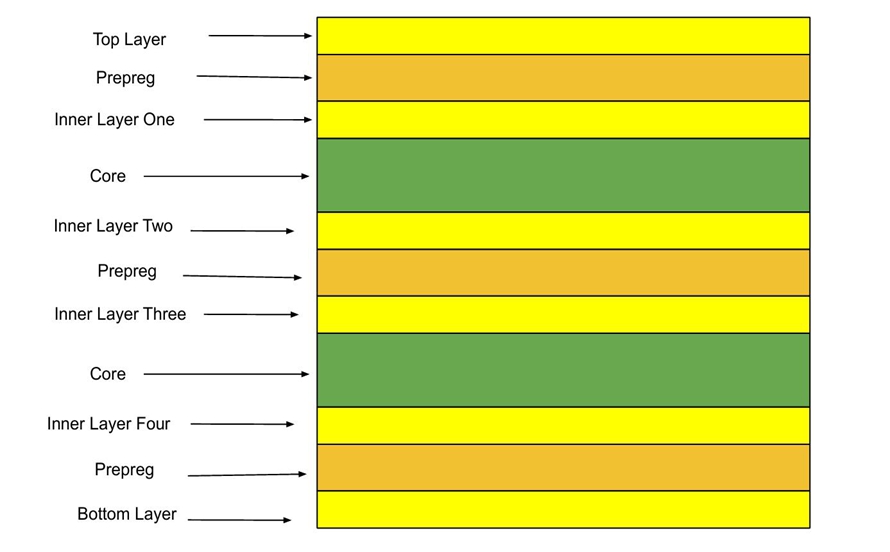
Start with a solid layer stackup, allocating inner layers to solid power and ground planes adjacent to signal layers for tight coupling. In compact boards, use microvias or blind vias to connect planes without consuming surface area. Avoid splits longer than a wavelength at operating frequencies to prevent slot antennas; instead, use stitching vias every lambda/20. Power plane design for compact boards benefits from poured copper fills on signal layers to extend effective plane area. Maintain at least 20% clearance around cutouts to preserve current flow uniformity. Simulate plane resonance modes early to adjust stackup.
For multilayer boards under four layers, dedicate one full plane to power and pair it with ground on the opposite side. Copper balancing prevents warpage, distributing weight evenly across the small footprint. Integrate thermal reliefs judiciously to avoid resistance spikes. These practices align with IPC-2221B for reliable power distribution. Testing via TDR confirms plane integrity post-fabrication.
Optimizing Decoupling Capacitor Placement
Decoupling capacitor placement near power pins minimizes loop area, reducing inductive voltage spikes. Position ceramics within 1-2 mm of IC balls or pads, prioritizing high-di/dt nets like clock drivers. Use a mix of values: 0.1 uF for mid-freq, 1-10 nF for GHz, and bulk 10-100 uF for low-freq. In small PCBs, array capacitors in a grid pattern under BGAs to cover the die shadow. Via-in-pad or embedded caps save space while maintaining efficacy. PDN impedance in small PCBs drops significantly with this distributed approach.
Vias must be paired: one to power plane, one to ground, as close as possible. Avoid routing signals over cap pads to prevent coupling. For dense areas, share vias between multiple caps to economize. Simulate placement sensitivity to confirm ripple suppression. Troubleshooting poor decoupling often traces to via inductance exceeding plane spreading.
Strategies for Minimizing Voltage Drop
Voltage drop in PDN traces follows Ohm's law, scaling with current density and length. Widen power traces proportionally to Irms, using IPC-2152B charts for cross-section adequacy under temperature rise limits. Planes inherently offer lower gradient due to parallel paths. In compact boards, segment planes with necked sections only where necessary, stitching across to equalize potential. Monitor gradient with Kelvin sensing in prototypes. These steps ensure components receive nominal voltage margins.
Bulk capacitance at board edges handles inrush, while local decoupling smooths transients. Fusing protects against shorts without excessive drop. Layer sequencing places high-current planes centrally for symmetry.
Leveraging Power Integrity Simulation for Custom PCB Sizes
Power integrity simulation verifies PDN performance before layout finalization, modeling custom PCB sizes accurately. Import stackup and geometry into PI tools to extract RLGC matrices. Sweep frequencies to check target impedance compliance, identifying hotspots. Time-domain IR drop analysis predicts worst-case droop during switching events. Adjust decoupling iteratively based on results. For small PCBs, 3D field solvers capture via and plane interactions precisely.
Include parasitics from connectors and loads for holistic views. Co-simulate with SI to catch crosstalk. Validation against measurements refines models. Power integrity simulation for custom PCB sizes prevents costly respins.
Conclusion
Effective PDN design in small PCBs hinges on low impedance, strategic decoupling, robust planes, and simulation-driven validation. Engineers balancing density with integrity achieve stable operation through disciplined practices. Key takeaways include adjacent plane pairing, grid decoupling, and impedance targeting. Custom sizes demand foresight to minimize voltage drop and ensure scalability. Implementing these elevates design reliability, meeting performance in ever-shrinking form factors.
FAQs
Q1: How does PDN impedance in small PCBs affect high-speed signal integrity?
A1: PDN impedance in small PCBs creates noise if exceeding target curves, coupling into signals via shared return paths. High impedance amplifies ripple, degrading eye height and increasing bit errors. Proper decoupling and plane design suppress this, maintaining clean references. Simulation confirms margins before fabrication.
Q2: What are key factors in decoupling capacitor placement for compact boards?
A2: Optimal decoupling capacitor placement positions caps closest to IC power pins, minimizing ESL loops with short vias to planes. Use value hierarchies for broadband coverage. In dense layouts, grids under packages ensure uniformity. Verify via PI tools for effectiveness.
Q3: How to implement power plane design for compact boards effectively?
A3: Power plane design for compact boards uses solid inner layers with stitching vias to avoid splits. Balance copper for flatness, pair Vcc/GND tightly. Clear cutouts strategically. Follow stackup symmetry for controlled impedance.
Q4: Why is power integrity simulation essential for custom PCB sizes?
A4: Power integrity simulation for custom PCB sizes models unique geometries, predicting droop and resonance unavailable analytically. It optimizes decoupling and traces iteratively. Early detection avoids respins, ensuring voltage stability across loads. Correlate with bench tests for accuracy.
References
IPC-2221B — Generic Standard on Printed Board Design. IPC, 2003
IPC-2152B — Standard for Determining Current Carrying Capacity in Printed Board Design. IPC, 2019
IPC-6012E — Qualification and Performance Specification for Rigid Printed Boards. IPC, 2017