ALLPCB


Introduction
If you are dipping your toes into PCB design as an electronic hobbyist, choosing the right surface finish can make or break your project. ENIG PCB finishing stands out as the gold standard because it combines reliability with ease of use for soldering and long-term storage. This guide breaks down ENIG PCB explained in simple terms, covering what it is, how the process works, and why it suits beginners building prototypes or custom circuits. Unlike rougher finishes that complicate hand soldering, ENIG provides a smooth, durable surface that protects your copper traces. By the end, you will understand ENIG PCB benefits and when to specify it for your next board. Let’s explore why this finish earns its reputation in the PCB world.
What Is ENIG PCB Finishing?
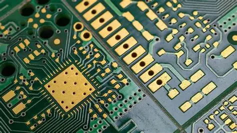
ENIG stands for Electroless Nickel Immersion Gold, a two-layer metallic coating applied to the exposed copper on a PCB. The first layer is electroless nickel, deposited without electricity through a chemical reaction, acting as a barrier against oxidation. A thin immersion gold layer then covers the nickel, providing corrosion resistance and excellent solderability. This combination makes ENIG ideal for what is ENIG PCB questions from newcomers, as it ensures pads remain usable even after months in storage. Hobbyists appreciate its flat surface, which supports precise soldering of surface-mount components without bridging issues. Standards like IPC-4552 define the requirements for this finish to ensure consistent quality across manufacturers.
ENIG differs from other finishes by using chemical deposition rather than hot air or immersion alone. The nickel layer is robust enough to handle multiple reflow cycles, while the gold ensures quick wetting during soldering. For beginners, this means fewer failed joints and less frustration during assembly. The process aligns with factory practices but scales well for small prototype runs common in hobby projects. Understanding this structure helps you specify ENIG confidently in your design files.
The ENIG PCB Process: Step by Step for Beginners
The ENIG PCB process starts with thorough cleaning of the PCB to remove oils, oxides, and residues from the copper pads. Micro-etching follows to create a fresh surface for plating adhesion. Activation with a catalyst, often palladium, prepares the copper for the electroless nickel bath. In the nickel plating step, a chemical reduction deposits a uniform nickel layer over all exposed copper areas.
Next comes the immersion gold stage, where gold displaces a tiny amount of nickel to form a protective topcoat. Rinsing and drying complete the sequence, preventing contamination between steps. This electroless method ensures even coverage on complex board geometries, unlike electrolytic processes that need electrical contacts. Hobbyists benefit from this uniformity, as it reduces variability in home soldering setups. The entire ENIG PCB process follows controlled chemistry to meet standards such as IPC-6012 for rigid board performance.
Factories monitor bath chemistry closely to avoid defects, but the result is a finish ready for immediate use. Beginners can visualize this as dipping the board through a series of chemical tanks, each building the protective layers. Patience in processing yields boards that withstand handling and environmental exposure.
ENIG PCB Benefits: Why It’s Perfect for Hobby Projects
One key ENIG PCB benefit is superior solderability, allowing solder to flow smoothly across pads for strong joints. The flat gold surface prevents the unevenness found in lead-free HASL finishes, making it easier to hand-solder fine-pitch parts like QFNs or BGAs. Corrosion resistance keeps copper safe from air and humidity, extending shelf life to over a year for stored prototypes. This matters for hobbyists ordering small quantities that sit between projects.
ENIG handles multiple thermal cycles well, resisting degradation during reflow soldering common in assembly. Its lead-free nature complies with modern environmental rules without sacrificing performance. Electrical conductivity remains high due to the noble gold layer, minimizing signal loss in high-frequency circuits. For beginners, these traits translate to reliable boards that perform as designed.
Another advantage is compatibility with wire bonding and press-fit connectors, opening doors to advanced hobby experiments. The finish maintains planarity under heat, avoiding warpage issues in multilayer boards. Overall, ENIG PCB benefits make it a versatile choice for everything from Arduino shields to custom audio amps.
Potential Challenges and Best Practices with ENIG
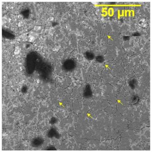
While ENIG shines, issues like black pad can arise from nickel corrosion under the gold, leading to poor solderability. This defect stems from excessive phosphorus in the nickel or aggressive gold immersion. Standards such as IPC-4552 include tests to detect and prevent black pad through proper thickness and purity controls. Hobbyists avoid this by choosing reputable fabricators who adhere to these guidelines.
Signal integrity concerns occur if nickel layers trap between traces, but proper design spacing mitigates this. For best practices, specify ENIG only on pads needing long-term protection, using cheaper finishes elsewhere if cost matters. Test solderability on samples before full assembly to catch any process variations. Storage in dry, anti-static bags preserves the finish’s integrity.
Monitoring reflow profiles prevents gold embrittlement, ensuring ductile joints. Beginners succeed by starting with simple single-sided boards to learn ENIG handling.
When to Choose ENIG for Your Electronic Projects
Opt for ENIG in projects with fine-pitch components or high-reliability needs, like sensors or RF modules. It outperforms HASL in flatness for BGA prototyping, reducing rework. For hobby audio or LED drivers, the corrosion resistance justifies the upgrade from basic finishes. Avoid it for very low-cost, high-volume throws where OSP suffices.
Compare to immersion tin: ENIG offers better shelf life but at higher cost. Wire bonding applications demand ENIG’s bond strength. Design tip: Mask non-pad areas to control finish application. This strategic use maximizes ENIG PCB benefits without overkill.
Conclusion
ENIG PCB finishing earns its gold standard status through unmatched solderability, flatness, and durability tailored for electronic hobbyists. From the electroless nickel base to the protective gold cap, the ENIG PCB process delivers boards ready for prototyping and beyond. Weigh benefits like long shelf life against practices to sidestep black pad. Specify it confidently for projects demanding precision. Your next custom circuit will thank you with reliable performance.
FAQs
Q1: What is ENIG PCB, and is it suitable for beginners?
A1: ENIG PCB is Electroless Nickel Immersion Gold, a surface finish with nickel and gold layers protecting copper pads. For beginners, it offers a flat, solder-friendly surface ideal for hand assembly and prototypes. Its long shelf life suits hobbyists storing boards. Widely adopted standards help ensure consistent quality.
Q2: What are the main ENIG PCB benefits for electronic hobbyists?
A2: Key benefits include excellent corrosion resistance, very flat pads for fine-pitch soldering, and stability across multiple thermal cycles. You get reliable joints, lead-free compatibility, and dependable performance for custom builds.
Q3: How does the ENIG PCB process work in simple terms?
A3: The board is cleaned and micro-etched, activated with a catalyst, plated with electroless nickel, then immersed in a gold bath that forms a thin protective layer. Rinsing between steps keeps the finish clean and uniform.
Q4: Can ENIG PCB cause issues like black pad, and how do you avoid them?
A4: Black pad is a defect from nickel corrosion that harms solderability. It’s avoided by controlling chemistry and thickness per industry specifications, choosing qualified fabricators, validating solderability on samples, and storing boards properly.