 ALLPCB


Introduction
PCB panelization combines multiple individual circuit boards into a single large panel to streamline manufacturing and assembly processes. This approach enhances efficiency by allowing high-volume production runs, reducing setup times, and optimizing material usage. In high-density designs, where components pack tightly and features like microvias demand precision, panelization introduces unique design for manufacturability (DFM) challenges. Engineers must balance cost savings with risks such as mechanical stress, thermal inconsistencies, and electrical interference. Proper panelization strategies ensure reliable yields while meeting stringent performance requirements. This article explores these challenges and provides structured solutions tailored for high-density PCB panelization.
Understanding PCB Panelization and Its Role in DFM
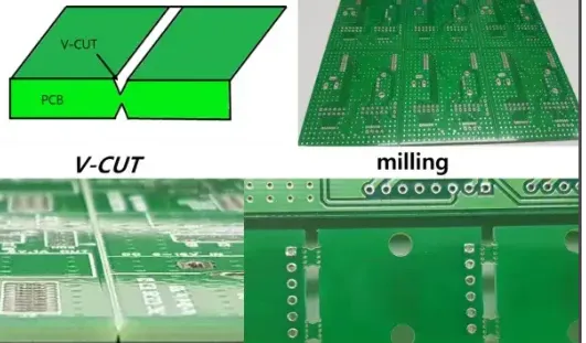
PCB panelization involves arranging multiple boards on a carrier panel, connected via methods like V-scoring or tab routing, before depaneling into singles. V-scoring creates partial cuts along straight lines for clean separation, ideal for rectangular boards, while tab routing uses perforated tabs for irregular shapes. Fiducial marks on panels aid machine vision for precise alignment during assembly. For DFM, panelization minimizes waste and supports automated handling, but high-density configurations amplify issues like board warpage and component shift. Adhering to standards like IPC-2221 ensures designs accommodate fabrication tolerances. Ultimately, thoughtful panelization directly impacts yield rates and long-term reliability in complex electronics.
High-density PCB panelization matters because modern devices demand smaller footprints with finer features, pushing panel densities higher. More boards per panel cut costs, but increase handling stresses and process variations. Electrical engineers must evaluate panel size limits, typically dictated by equipment capabilities, to avoid defects. Poor planning leads to scrap from misalignment or damage during depaneling. Effective DFM integrates panelization early in the design phase, aligning with fabrication capabilities for optimal outcomes.
Key Challenges in High-Density PCB Panelization
High-density PCB panelization faces mechanical hurdles from increased board counts and tighter spacing. Thinner substrates and dense copper pours heighten warpage risks during lamination and reflow, as uneven thermal expansion stresses the panel. Depaneling forces propagate cracks or delamination if scores or tabs lack reinforcement. Engineers observe these effects more in panels exceeding standard sizes, necessitating simulations for stress distribution. Material selection influences outcomes, with low-CTE laminates mitigating distortions. Addressing these ensures structural integrity across the production flow.
Fine-pitch component panelization complicates stencil printing and pick-and-place operations. Components with 0.3 mm or smaller pitches require sub-micron registration across the entire panel, where cumulative tolerances from panel flex or fiducial misalignment accumulate. Solder paste volume variations arise from panel bow, leading to bridging or insufficient joints. High-density arrays exacerbate stencil liftoff issues due to shared edges. Validation through shadow moire analysis helps quantify these distortions pre-production. Precise fiducial placement and rigid panel frames counteract these effects effectively.
Thermal management in PCB panels demands uniform heat distribution to prevent hotspots in dense layouts. High-power components clustered near panel edges experience uneven reflow profiles, causing voids or head-in-pillow defects. Panel size influences oven zoning, with larger arrays requiring slower ramp rates per IPC guidelines for thermal uniformity. Copper imbalance between boards induces differential expansion, stressing vias and traces. Embedded thermal planes help, but panel-level simulations predict gradients accurately. Proactive stackup symmetrization across the panel maintains process windows.
Signal integrity panelization issues stem from crosstalk between adjacent boards sharing common ground planes or power rails. High-speed signals on fine lines couple electromagnetically through panel gaps, degrading eye diagrams. Return path discontinuities at score lines disrupt impedance control, especially in differential pairs. Dense routing amplifies stub effects during depaneling if tabs interrupt shields. Controlled impedance verification on paneled prototypes reveals these anomalies early. Strategic spacing and ground stitching minimize propagation delays and jitter.
Minimizing EMI panelization requires isolating emissions from densely packed boards. Radiated interference couples via panel slots or flexing during handling, violating compliance thresholds. Fine-pitch vias act as antennas if not suppressed, particularly in HDI layers. Edge plating or shielding fences between boards contain fields effectively. Compliance testing on full panels identifies resonances before singles. Layout symmetry and guard traces further reduce susceptibility.
Complex PCB shape panelization relies on tab routing for non-rectangular outlines, introducing stress concentrations at tab locations. Irregular contours demand mouse bites or perforations, risking microcracks in brittle high-density substrates. Fiducial optimization ensures router accuracy amid shape variations. Thicker tabs with fillets distribute forces evenly during separation. Hybrid V-score and routing combinations suit hybrid shapes, balancing efficiency and precision.
Rigid-flex PCB panelization handles dynamic regions carefully to avoid flex damage during rigid board processing. Flex tails must align without torsion, as panel stresses propagate to bends. Coverlay alignment across panels challenges lamination registration. Depaneling methods avoid scoring through flex zones, favoring laser or mechanical routing. Stackup transitions require reinforced tabs for handling stability.
HDI PCB panelization integrates microvias and blind vias, per IPC-2226, complicating laser depaneling to preserve via integrity. Stacked vias near edges risk aspect ratio violations from panel tolerances. Fine-line etching uniformity suffers in large panels due to etch factor variations. Build-up processes demand sequential panel checks for layer alignment.
Best Practices for Overcoming Panelization Challenges
Start with panel layout optimization, maximizing board count while maintaining 5 mm borders for clamping. Simulate warpage using finite element analysis to predict bow under thermal loads. Symmetrical arrangements equalize stresses, reducing deviations below 0.75% per industry benchmarks. Incorporate breakaway rails with fiducials at corners and centers for multi-zone registration.
For fine-pitch component panelization, use high-precision fiducials with 0.1 mm tolerances, placed asymmetrically to detect rotation. Stiffener frames prevent bow during printing, ensuring paste height consistency. Validate with SPI on paneled arrays before reflow.
Thermal management in PCB panels improves via balanced copper distribution and thermal vias linking planes. Panel breakouts for thermocouples monitor profiles in qualification runs. Select low-Dk materials for uniform reflow, adhering to J-STD-020 for moisture sensitivity.
Signal integrity panelization benefits from 2 mm minimum spacing between boards, with grounded guard rings along edges. Verify S-parameters on test coupons embedded in panels. Controlled depth routing preserves dielectric integrity.
To minimize EMI panelization, add edge castellations or moats separating boards electrically. Enclose panels in Faraday frames during test. Layer shielding with via fences blocks coupling paths.
Complex PCB shape panelization employs optimized tab patterns: 3-5 mm wide, spaced 10-15 mm apart, with 0.5 mm mouse bites. Fillet radii at roots prevent tear-outs. Toolpath planning avoids dwell marks on traces.
Rigid-flex PCB panelization uses dedicated carriers for flex sections, with tabs only on rigid portions. Laser trimming post-flex processing preserves bend radii per IPC-2223.
HDI PCB panelization favors laser depaneling for clean edges, minimizing heat-affected zones near microvias. Sequential build-up with interim inspections controls stack tolerances.
Troubleshooting Common Issues
Warpage exceeds limits: symmetrize stackups, add constraint vias. Fine-pitch bridging: refine stencil apertures, use low-residue paste. SI degradation: increase inter-board gaps, review return paths. EMI failures: implement shielding, retest on panels.
Conclusion
High-density PCB panelization demands meticulous DFM to navigate mechanical, thermal, and electrical challenges. From fine-pitch alignment to HDI via preservation, structured approaches yield robust designs. Integrating simulations, standards compliance, and best practices ensures high yields and performance. Electrical engineers benefit from early collaboration with fabricators. Mastering these elements unlocks efficient production for advanced applications.
FAQs
Q1: What are the main challenges in high-density PCB panelization?
A1: High-density PCB panelization struggles with warpage from thermal mismatch, alignment errors for dense fiducials, and stress during depaneling. Adjacent boards risk crosstalk and EMI coupling due to tight spacing. V-scoring suits rectangles but limits complex shapes, while tab routing adds handling complexity. Simulations and balanced layouts mitigate these logically.
Q2: How does thermal management in PCB panels affect DFM?
A2: Thermal management in PCB panels requires uniform reflow to avoid defects like voids in high-density areas. Larger panels demand adjusted oven profiles for even heating. Copper balancing and vias distribute heat effectively. Per standards, monitoring prevents hotspots, ensuring reliable solder joints across the array.
Q3: What best practices address signal integrity panelization?
A3: Signal integrity panelization improves with 2 mm+ spacing, ground stitching, and impedance-controlled edges. Embed test coupons for S-parameter checks on panels. Guard traces block crosstalk from shared paths. This structured method preserves high-speed performance post-depaneling.
Q4: Why is rigid-flex PCB panelization more complex?
A4: Rigid-flex PCB panelization protects flex zones from rigid processing stresses, using selective tabs and carriers. Alignment challenges arise at transitions. Laser methods preserve integrity without scoring flex. Following design standards ensures scalability for high-density hybrids.


